Method and circuit for setting and reading unique identification code of chip on silicon wafer in batch

An identification code and chip technology, applied in the field of chip programming, can solve the problems of increasing cost, trouble, and incompatibility with standard processes, and achieve the effects of extending life, reducing costs, and reducing deformation and wear.

Inactive Publication Date: 2010-06-23
SICHUAN KILOWAY ELECTRONICS
0 Cites 9 Cited by

AI-Extracted Technical Summary

Problems solved by technology

This method is also cumbersome to operate in terms of technology. Due to the insertion and modific...

Method used

In addition, in the present invention, block adopts shared programming soldering pad, and probe is not contacted with chip during programming, can not bring pin mark to soldering pad, bump or planting ball, also reduces chip pollution Chance. Moreover, the invention provides an electrostatic protection circuit at the common programming pad, so that the entire block can share the electrostatic protection circuit, thereby providing electrostatic protection for the programming port of each chip without occupying the chip area, which has higher cost efficiency ratio, which is conducive to improving the yield. Moreover, because the present invention does not need to arrange test pads on the chip, the shielding mask is omitted, and the cost of the packaging process is reduced.
One: the ROM method is set. By adopting the method of setting the mask-type read-only memory, a block of the mask-type read-only memory of a low-end bit string is spliced ​​with the layout of the main chip. In the case that the low-end bit string is relatively short, considering that the length of the low-end bit string is short and does not require random access, the decoder can be omitted, and the sequential reading method is adopted, from high to low or from low to high The order of reading the low-end bit strings in order to simplify the structure. Or connect all bits of the low-end bit string in parallel to a digital circuit, and the digital circuit acts as a port to read in parallel.
Utilize the hardware structure of the present invention, complete the programming of a chip from a group of probes, a group of channels, a programming operation process and improve to a group of probes, a group of channels, a programming operation process to complete the chip programming of a block , not only saves the programming time of each chip, but also saves the stepping time of each probe card. For a block of 1024 chips, if its single chip programming time is 15 milliseconds, and the probe stepping time is 0.4 seconds, then according to traditional programming, the total time is 424.96 seconds. If the bit string is programmed in parallel, the conversion time can be reduced to less than 0.415 seconds, and the programming speed is increased by 1024 times. For a silicon wafer with 65536 chips, it takes 7.6 hours to program according to the traditional method, but it can be shortened to 26 seconds by parallel programming. The improvement of programming speed reduces the occupation time of programming equipment and greatly reduces the program...

Abstract

The invention discloses a method for setting unique identification code of chip on silicon wafer in batch which includes the steps: dividing the chip on the silicon wafer into a plurality of blocks; dividing the bit of the chips into LBS and HBS according to the quantity of chip in one block, setting LBS by taking the chips as unit and uniformly setting the numerical value of HBS of the chips in the blocks by taking blocks as unit; and setting the unique identification code. The invention also discloses a method for reading the unique identification code to respectively read the LBS and HBS of the unique identification code and combine the two into a complete unique identification code, or directly read the unique identification code when the HBS and LBS of the unique identification code in the chip are neighboring and ordered. The hardware structure of the invention divides one silicon wafer into a plurality of blocks; each chip in each block shares programmable interconnection, input/output solder pad, probe card and programmable equipment channel. The invention can improve high programming speed, reduce cost and improve yield by setting high-end bit string in the chips.

Application Domain

Semiconductor/solid-state device manufacturingRecord carriers used with machines

Technology Topic

Silicon chipInput/output +5

Image

  • Method and circuit for setting and reading unique identification code of chip on silicon wafer in batch
  • Method and circuit for setting and reading unique identification code of chip on silicon wafer in batch
  • Method and circuit for setting and reading unique identification code of chip on silicon wafer in batch

Examples

  • Experimental program(1)

Example Embodiment

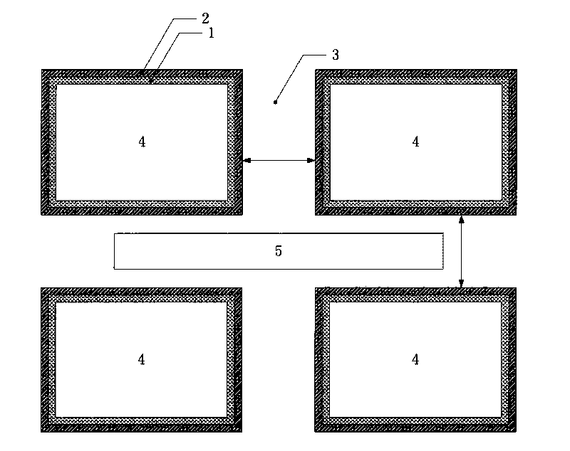
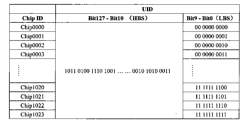
[0036] Observing the arrangement of the UID coded bit string within a certain range, it can be found that: in the UID coded bit string with m bits long and k continuous, the highest bit is defined as the k-1 bit and the lowest bit is the 0th bit. n, first obtain N by finding the logarithm of m with base 2 as N, N=Log(2)m, when N is an integer, n=N, when N is a decimal, n is rounded up to N, n= floor(N), at this time, taking the nth bit as the boundary, in the m unique identification code coded bit strings, the nth bit to the m-1th bit are the same, and the 0th bit to the n-1th bit It changes in increasing or decreasing order. In the coded bit string that defines the unique identification code, the 0th bit to the n-1th bit is the Low End Bit String (LBS), and the nth bit to the m-1th bit is the high-end bit string ( High End Bit String, referred to as HBS).
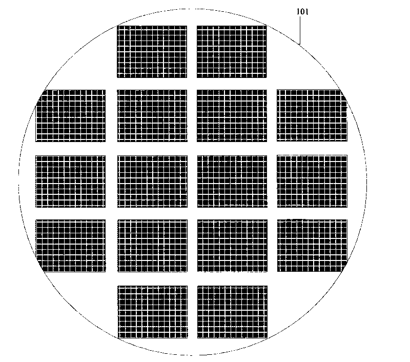
[0037] Such as image 3 As shown, a string of 128-bit unique identification codes, the lowest bit is the 0th bit, and the highest bit is the 127th bit. When the number of chips is 1024, that is, m=1024, calculate n according to the formula, n=log(2)1024, and get n=10. Among the user coded bit strings in these chips, the high-end bit string is from each chip The 10th to 127th bits of the encoding, and the low-end bit string is the 0th to 9th bits of each chip encoding. Then the high-end bit string part of the UID code of this internal chip, that is, the 127th to the 10th bit are the same, and the low-end bit string part, that is, the 9th to the 0th bit, is incrementally changed from 0000 to 1023 .
[0038] Such as Picture 9 As shown, the method for editing the unique identification code in the chip of the present invention includes the following steps:
[0039] First, divide a wafer into multiple blocks. The main considerations when dividing a silicon wafer into multiple blocks include chip size, photolithography window size, dicing slot size, semiconductor foundry or wafer foundry test pattern requirements, parallel programming drive current load and other parameters. Therefore, the number of blocks divided by a silicon wafer is determined according to specific needs. After the silicon chip is divided into blocks, each block contains m chips, and m is of course a natural number greater than 1. In this embodiment, one block contains 1024 chips, that is, m=1024.
[0040] Secondly, on the basis of dividing the silicon chip into blocks, according to the number m of chips included in a block, the unique identification code bit string in the chip is divided into a high-end bit string and a low-end bit string. Specifically, this is done. First, the boundary position n between the high-end bit string and the low-end bit string is obtained by the number m of chips included in each block. In the process of finding n, first find the logarithm of m with base 2 to get N, N=Log(2)m, if N is an integer, then n=N, if N is a decimal, then the value of n is N Round up and add 1, that is, if n is N, round up, n=floor(N). Calculate the logarithm of 1024 with the base of 2, and get N=10, so n=N=10. That is, in this embodiment, in the chip's unique identification code encoding bit string, the high-end bit string and the low-end bit string are separated by the 10th bit.
[0041] Third, the unique identification code is divided into a high-end bit string and a low-end bit string using n as the boundary. When the bit length of the chip is k, the highest bit is the (k-1)th bit, the lowest bit is the 0th bit, and the lowest bit of the chip is the low-end bit string from the 0th bit to the (n-1)th bit. Consecutive codes from bit to the highest bit (k-1) of the chip are high-end bit strings. In this embodiment, as image 3 As shown, the chip bit length is 128, the highest bit is the 127th bit, and the lowest bit is the 0th bit, then the low-end bit string from the 0th to the 9th bit, and the high-end bit string from the 10th to the 127th bit. The high-end bit string and the low-end bit string are combined into a unique identification code.
[0042] Then, the low-end bit string and the high-end bit string are respectively set.
[0043] The first is to set the low-end bit string of each chip in chip units. The values ​​of the low-end bit string from the 0th bit to the 9th bit from the 1st chip to the mth chip correspond to 0 to m-1 in sequence. That is image 3 As shown, the value of the low-end bit string of the first chip is 0, the value of the low-end bit string of the first chip is 0, the value of the low-end bit string of the first chip is 0, and the value of the second chip is 0. The value of the low-end bit string is 1, the value of the low-end bit string of the third chip is 2, ... the m-th, that is, the value of the low-end bit string of the 128th chip is m-1, which is 127. These values ​​are represented by binary numbers in the chip, which are 0000000000, 0000000001, 0000000010, ... 11111111111. The value of the low-end bit string of each chip logically corresponds to the chips contained in this block one-to-one. Therefore, the low-end bit string of each chip is set in chip units.
[0044] Then, the high-end bit strings of all chips in a block are set in units of blocks. Because as image 3 As shown, when the number of chips is 1024 (m=1024), the high-end bit string part (bit 127 to bit 10) of the UID code of the chip is the same. Take the block as the unit to uniformly set the value of the high-end bit string of the chip in the block.
[0045] Finally, according to the unique identification code encoding characteristics, since the m chips have been preset with low-end bit strings, as long as the high-end bit strings are written uniformly and in parallel during programming, the programming purpose of the unique identification code of the chip in the entire block can be completed. It can achieve the purpose of fast, parallel, and batch programming, and at the same time, it solves the contradiction between the chip pattern replication and the UID differentiation of the replicated chip on the standard process flow.
[0046] When setting the low-end bit string of each chip in a block by chip as a unit, two methods can be selected: layout setting method and auxiliary circuit method.
[0047] The layout setting method is that in the post-processing of the layout, the chip that arranges the building blocks is not usually simply copied repeatedly, but is set by some methods, so that it has different low-end bit strings. Generally, on the basis of completing the main chip layout, part of the layout can be modified one by one, or a layout array of low-end bit strings can be pre-generated by manual or automated tools, and then combined with the main layout. For blocks with a reasonable size division and a limited number of chips, even if manual settings are used, the workload is still within the achievable or acceptable range. If automated design tools are used, it is more convenient and faster.
[0048] In the present invention, the following three implementation methods can be used to set the low-end bit string of each chip by using the layout:
[0049] One: Set the read-only memory method. The mask-type read-only memory is set up to make a low-end bit string of mask-type read-only memory blocks and the master chip layout. In the case that the low-end bit string is relatively short, considering that the length of the low-end bit string is short and does not require random access, the decoder can be omitted, and the sequential reading method can be used in order from high to low or from low to high Read the low-end bit string in sequence to simplify the structure. Or connect all the bits of the low-end bit string in parallel to the digital circuit, and the digital circuit is read in parallel as a port.
[0050] Two: Set up the connection method. This method further simplifies the physical realization method on the basis of setting the read-only memory method, such as Image 6 As shown, the digital circuit sequentially corresponds the low-end bit string of the chip to the n input ports of the digital circuit, and each low-end bit string is mapped to each port. By connecting the low-end bit string and the corresponding port respectively, according to the low-end bit string Serial coding connects the ports to high or low potentials to achieve settings. in Image 6 , The low-end bit string of the structure shown is 1010101010.
[0051] When setting the low-end bit string by setting the read-only memory method and setting the wiring method, there are two ways to set the unique identification code: 1. Connect the set low-end bit string as an independent port to the application circuit to set the chip unique For the low-end bit string of the identification code, the chips in one block in the set high-end bit string are written into the same high-end bit string in parallel, and at this time, the chips in one block are written into the same high-end bit string in parallel. When the unique identification code set in this way is used, if the unique identification code is read, the high-end bit string and the low-end bit string in the unique identification code encoding are combined into a complete unique identification code and read directly. Two: Copy the low-end bit string of each chip set in a block, and merge with the set high-end bit string to form a unique identification code, and write the unique identification code into the programmable memory. When setting the unique identification code in this way, if it is necessary to read the unique identification code code, just read the unique identification code code directly.
[0052] Three: Short-circuit or disconnect the memory cell method. Such as Figure 7 As shown, word lines include w0 to w3, and bit lines include b0 to b3, Figure 7 The input and output of the unit shown in the figure are forcibly short-circuited, and the output result is forced to 1, while the output result of the unit that is not forcibly short-circuited is determined by the data stored in the storage unit. By finding the unit corresponding to the storage address of the low-end bit string in the programmable memory, short-circuit or disconnect the modification, and forcibly change the output of these bits. After setting in this way, the memory data bit corresponding to the low-end bit string should no longer be programmed. When the low-end bit string is set in this way, the same high-end bit string is directly written to each chip in a block, and the low-end bit string is no longer programmed. When reading the unique identification code, read the high-end bit string and the low-end bit string separately, and then combine the high-end bit string code and the low-end bit string code into a complete unique identification code code. If the high-end bit string and the low-end bit string are adjacent and in sequence, just read the unique identification code directly.
[0053] The auxiliary circuit rule is to use some auxiliary logic or analog circuits to generate the low-end bit string value, and then input the corresponding chip as a reference, so as to achieve the purpose of setting the low-end bit string. This method is simpler and more reliable than the layout method. Such as Figure 8 As shown, the low-end bit string of the 0th chip is 0000, and an adder is set in the dicing slot between the 0th chip and the first chip to add the value of the 0th chip's low-end bit string 1. Obtain the low-end bit string value of the first chip 0001, and then set an adder in the dicing slot between the first chip and the second chip to add the low-end bit string value of the first chip Add 1 to get the low-end bit string value 0002 of the second chip, and so on, set an adder in the dicing slot between the 0th chip and the 1st chip to add the value of the h-1th chip Add 1 to the value of the low-end bit string to get the low-end bit string value of the h-th chip 000h. Finally, connect m-1 n-bit adders in series, and set the first-level chip input to 0, and each level of adder Add 1 on the basis of the previous level, and the output of each level of adder is used as the low-end bit string value input of a chip, that is, the output of the adder from level 0 to m-1 is used as the 0th to m-1th Input of the low-end bit string of a chip. After power-on, the adders of all levels will be added level by level. After a certain period of time is stable, the low-end bit string value of each level of chip is obtained. Then, each chip needs to write the low-end bit string value into the programmable non-volatile memory to solidify it through a programming operation.
[0054] When the auxiliary circuit method is used to set the low-end bit string encoding of the unique identification code of each chip, there are two ways to set the unique identification code encoding: one: first transmit the value of the high-end bit string when setting, and the chip will set the high-end bit string and the low The terminal bit string is combined into a unique identification code, and then written into the programmable memory. The unique identification code set in this way is used to directly read the unique identification code when reading. Two: Program the high-end bit string uniformly according to the matrix, and write the low-end bit string of each chip according to the output value of the corresponding adder. With the unique identification code set by this method, when reading, the high-end bit string and the low-end bit string are read respectively, and then the two are combined into a complete unique identification code. When the high-end bit string and the low-end bit string are connected and in sequence, the unique identification code can be directly read.
[0055] It can be seen from the above process that the setting of the low-end bit string code ensures that the unique identification codes of the chips in a block are different, and each block uses a unique high-end bit string code to ensure unique identification between blocks. Code difference. Therefore, as long as it is ensured that the high-end bit strings of all blocks are different throughout the life of the product, it can be guaranteed that all chips produced have a unique unique identification code.
[0056] In the invention, various programmable memories can be used as unique identification code data carriers, combined with a programmable memory compatible with standard CMOS technology to set the unique identification code of the chip. It can also realize the programming of the chip's initialization data on the silicon chip, or use the set low-end bit string alone as the chip selection ID of the bus system to form the basis of silicon automatic testing or other silicon-level chip communication.
[0057] Because in the present invention, the hardware structure used for programming also includes programming connections, input/output pads, probe cards and programming device channels, since each chip in a block is written with the same high-end bit string, The high-end bit string of the chip is programmed in parallel, such as Figure 4 , 5 As shown, programming connections, input/output pads, probe cards, and programming device channels can all be shared. When the silicon wafer is divided into multiple blocks, the total size of each block plus the surrounding dicing groove is smaller than the light Engraved window size.
[0058] With the above structure, the high-end bit string of the block can be programmed in parallel, which greatly improves the programming speed. The programming wiring and the programming auxiliary circuit are located in the dicing slot in a block, and the test pattern set by the silicon wafer factory is located in the dicing slot between the blocks. An electrostatic protection circuit can also be provided at the input/output pads of a block.
[0059] The high voltage used for programmable memory programming can come from a built-in charge pump or an external input. For the device identification chip with on-site programming function, the built-in charge pump can be used; for the read-only radio frequency identification chip, because the charge pump needs to occupy a large chip area, additional circuit design is required. Therefore, the external input is more Suitable. According to the formula power P=voltage U*current I, under the same programming power, increasing the input voltage is beneficial to reduce the programming current. For example, for 1024 chip programming, if the memory cell programming voltage is 10v, the current is 200uA, if the external programming voltage is directly input 10v, the total programming current is 0.2A; if the 3.3v boost to 10v is used, the total programming The current is 0.62A. Considering the efficiency loss of the charge pump, the total current consumption may be more than 1A. It can be seen that the use of external high-voltage input can reduce the programming current, reduce the power line width, and improve the load capacity of the programming circuit.
[0060] When the silicon wafer is divided into multiple blocks, when one block is placed, it will be made into a photomask. There will be some other test patterns or marks around the photomask to verify whether the photomask is correct. When the silicon wafer is diced, the small units cut along the dicing groove are called the die, including layout, buffer, seal ring and dicing groove (scribe line) part. As for the wiring, circuit, and pad for programming the unique identification code, it generally only needs to be used once and will not be modified after programming, so this part of the module can be placed in a dicing block The slot area belongs to the user setting area. After programming, this part of the circuit or connection line is disconnected with the dicing, and UID can no longer be written or modified, which not only improves the security, but also saves the chip area.
[0061] Using the hardware structure of the present invention, the programming of a chip is improved from a set of probes, a set of channels, and one programming operation to a set of probes, a set of channels, and one chip programming is completed in one programming operation, which not only saves money It saves the time of chip-by-chip programming, and also saves the time of each probe card step and needle. For a block of 1024 chips, if the programming time of a single chip is 15 milliseconds and the probe stepping time is 0.4 seconds, then according to traditional programming, the total time is 424.96 seconds. If the hardware structure of the present invention is used for the high end of a block The bit string is programmed in parallel, and the time can be reduced to less than 0.415 seconds, and the programming speed is increased by 1024 times. For a silicon wafer with 65536 chips, programming according to the traditional method requires 7.6 hours, while parallel programming can be shortened to 26 seconds. The increase in programming speed reduces the time spent on programming equipment and greatly reduces programming costs. At the same time, as the product production cycle is shortened, it also brings advantages in product launch speed, output, and total cost. Moreover, the present invention also reduces the deformation and wear of the probe and prolongs the life of the probe card. Although parallel programming can also be achieved by using multi-point probe arrays in the prior art, the scale of parallel programming is greatly restricted due to the number of programming equipment channels and the limitations of the probe card technology. For parallel programming of chips, the equipment required will be very expensive. In addition, the programming device may not use a dedicated silicon chip-level chip test system. A set of probe card, microscope, microcontroller (MCU) and a few accessory parts can realize a simple silicon-level UID setting and chip test system.
[0062] In addition, in the present invention, a common programming pad is used for the blocks, and the probe does not contact the chip during programming, which will not bring pin marks to the pads, bumps or bumps, and also reduces the chance of chip contamination. Moreover, the invention is to install an electrostatic protection circuit at the common programming pad, so that the entire block can share the electrostatic protection circuit, so that the programming port of each chip can be provided with electrostatic protection without occupying the chip area, which is cost-effective Ratio, is conducive to improving the yield. Moreover, in the present invention, since there is no need to provide test pads on the chip, the shielding mask is omitted, and the cost of the packaging process is reduced.
[0063] In summary, compared with the traditional method, the editing method of the unique identification code in the RFID chip of the present invention achieves better results in terms of programming speed, programming cost, flexibility, and process compatibility, and has the following advantages: It is cost-effective, compatible with standard process flow, greatly improves the speed and efficiency of programming, saves chip area, reduces the requirements for programming equipment, improves anti-tampering ability, and simplifies subsequent packaging procedures.
[0064] The present invention can adopt various programmable memories as UID data carriers. For example, when combined with programmable memories compatible with standard CMOS (Complementary Metal-Oxide Semiconductor) technology, it is an ideal chip UID setting solution. The invention can be extended to realize the programming of the initialization data of the chip on the silicon chip. In addition, the LSB set according to the description of the present invention can also be used alone as the chip selection identification code of the bus system to form the basis of silicon-level automatic testing or other silicon-level chip communication. The invention can be applied to all chips that need to set a unique identification code of the chip.

PUM

no PUM

Description & Claims & Application Information

We can also present the details of the Description, Claims and Application information to help users get a comprehensive understanding of the technical details of the patent, such as background art, summary of invention, brief description of drawings, description of embodiments, and other original content. On the other hand, users can also determine the specific scope of protection of the technology through the list of claims; as well as understand the changes in the life cycle of the technology with the presentation of the patent timeline. Login to view more.

Similar technology patents

Method for measuring particle size distribution of particles, and apparatus thereof

InactiveCN103983546Aacceleratelower requirement
Owner:INST OF HIGH ENERGY PHYSICS CHINESE ACADEMY OF SCI

Method and device for quickly inquiring and calculating MangoDB cluster

InactiveCN103207919Aaccelerate
Owner:BEIJING IZP NETWORK TECH CO LTD

Method for data migration of non-relational database HBase

InactiveCN103514274AaccelerateEnsure data consistency
Owner:NINGBO DONGGUAN TECH

Classification and recommendation of technical efficacy words

  • accelerate
  • low cost

Three-dimensional circuit manufacturing process and composite components of laser plastic material and manufacturing method

ActiveCN101859613Aaccelerateaccelerated continuous motion
Owner:深圳市微航磁电技术有限公司

Failure recognition method and system based on neural network self-learning

ActiveCN103914735ASpeed ​​up fault identificationaccelerate
Owner:BEIJING TAILEDE INFORMATION TECH

Method and apparatus for loading web pages

ActiveCN101369284Ashorten the timeaccelerate
Owner:BEIJING SOGOU TECHNOLOGY DEVELOPMENT CO LTD

System and method for transmitting wireless digital service signals via power transmission lines

ActiveUS7929940B1reduce bandwidth requirementlow cost
Owner:NEXTEL COMMUNICATIONS

System and method for determination of position

InactiveUS20090149202A1low costreduce requirement
Owner:STEELE CHRISTIAN

Adaptive antenna optimization network

InactiveUS6961368B2low costminimal space
Owner:ERICSSON INC

Antenna device and method for attaching the same

ActiveUS20150138022A1low costimproved strength characteristic
Owner:NEC CORP
Why Eureka
Try Eureka