Groove type power MOS device with improved terminal protective structure

A technology of terminal protection structure and MOS device, applied in the direction of electric solid device, semiconductor device, semiconductor/solid state device components, etc., can solve the problems of waste, cost increase, increase device on-resistance, etc., to reduce complexity and difficulty degree, ensure the effect and stability, reduce the effect of die area

Active Publication Date: 2010-06-23
WUXI NCE POWER
View PDF2 Cites 11 Cited by
  • Summary
  • Abstract
  • Description
  • Claims
  • Application Information

AI Technical Summary

Problems solved by technology

This structure with extremely uneven distribution of electric field intensity may lead to premature breakdown of the MOS device in a local area when the forward bias voltage of the drain 14 is increased, deteriorating the breakdown performance of the device
[0005] 2. When a forward bias voltage is applied to the drain 14, the voltage of the MOS device is mainly composed of the cell trench 17 corresponding to the outermost cell area 1 and the voltage division protection area 2 corresponding to the cell area 1 When the P-well 7 between the voltage-dividing trenches 16 and the voltage-dividing protection region 2 correspond to the voltage-dividing trench 16 close to the cell region 1 for sharing, the remaining P-wells 7 on the voltage-dividing protection region 2 and the voltage divider groove 16 did not achieve the purpose of the voltage divider design, wasting the area of ​​the terminal protection area
For power MOS devices, the terminal protection structure occupies at least 20% of the die area, so the waste of area will lead to an increase in cost; if the total die area remains unchanged, the area of ​​the cell area must be sacrificed to make up, which will also increase Device on-resistance

Method used


Image

  • Groove type power MOS device with improved terminal protective structure
  • Groove type power MOS device with improved terminal protective structure
  • Groove type power MOS device with improved terminal protective structure

Examples


Embodiment Construction

[0023] The present invention will be further described below in conjunction with specific drawings and embodiments.

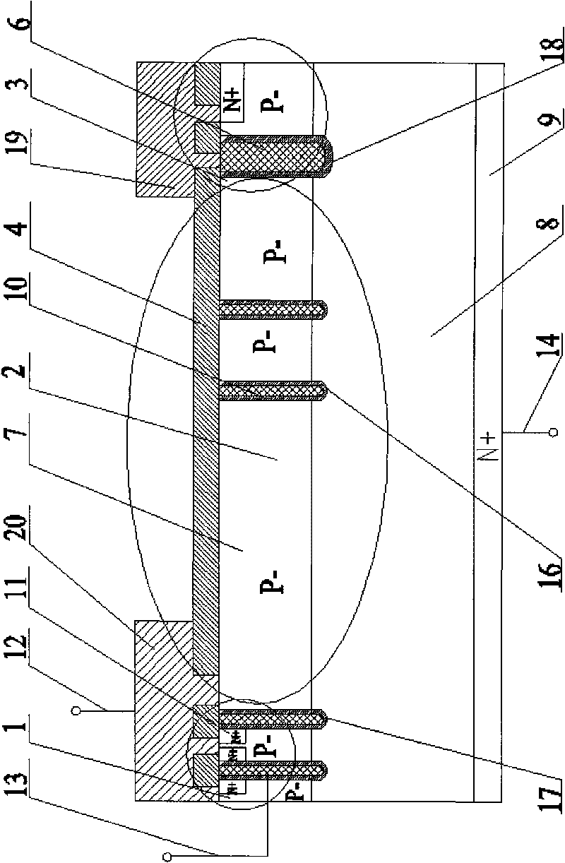
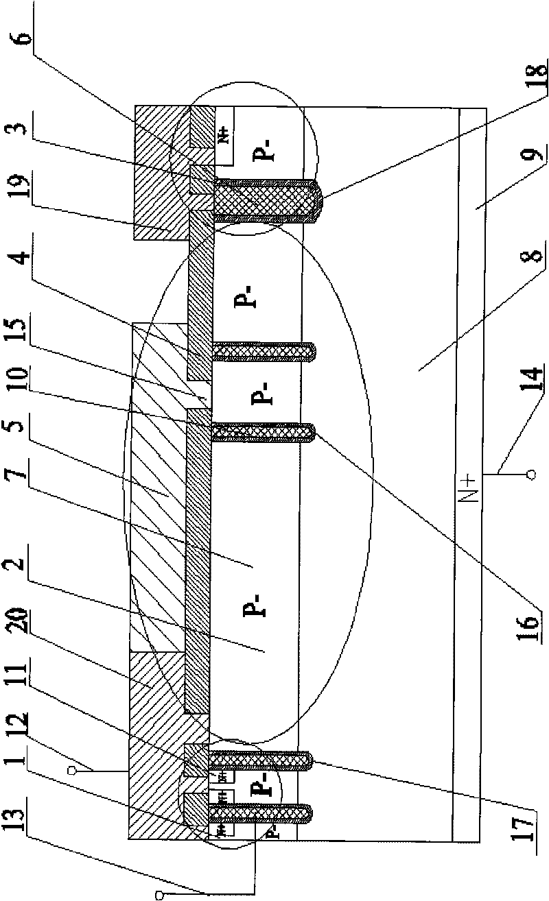
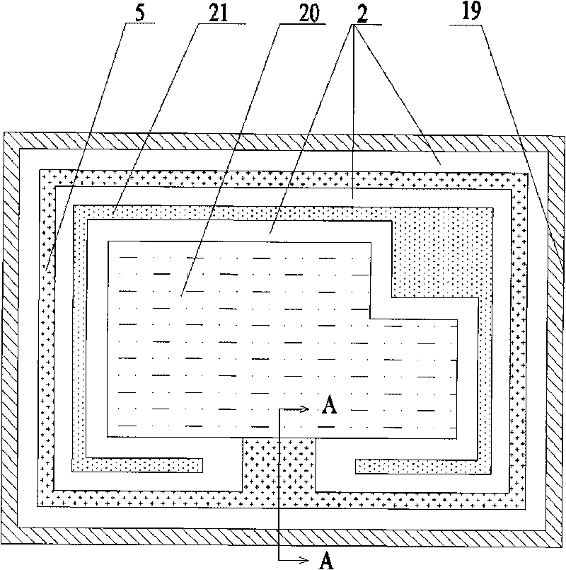
[0024] Such as Figure 2 ~ Figure 3 As shown: taking an N-type MOS device as an example, the present invention includes a cell area 1, a voltage division protection area 2, a cut-off protection area 3, an insulating dielectric layer 4, a first metal connection line 5, a conductive polysilicon 6, and a P-well 7 , N-type epitaxial layer 8, N+ substrate 9, insulating gate oxide layer 10, N+ implantation region 11, source terminal 12, gate terminal 13, drain terminal 14, ohmic contact hole 15, voltage dividing trench 16, cell trench 17. Stop trench 18 , second metal connection 19 , source metal 20 and gate metal 21 .

[0025] image 3 It is a metal wiring diagram of a deep trench high-power N-type MOS device overlooking the state plane. Such as image 3 As shown, the central region of the MOS device is the source metal 20, the cell region 1 is covered by the so...


PUM


Abstract

The invention relates to a groove type power MOS device, in particular to a groove type power MOS device with an improved terminal protective structure. A cellular area which is arranged on a semiconductor base plate and a terminal protective structure are arranged on the overlook surface of the MOS device, the cellular area comprises a plurality of cellulars which are connected in parallel and is arranged in the centre area of the semiconductor base plate; the terminal protective structure is arranged at the periphery of the cellular area, and the cellulars in the cellular area are connected to a whole body in parallel by an electro-conductive polycrystalline silicon which is arranged in the groove; the terminal protective structure comprises a partial pressure area which is arranged in the inner circle of the terminal protective structure and a cut off protective area which is arranged in the outer circle of the terminal protective structure; the partial pressure area adopts a groove structure, the groove structure comprises at least two partial pressure grooves, an ohmic contact hole is arranged between two adjacent partial pressure grooves, therefore, a second electro-conductive type layer which is arranged between two adjacent partial pressure grooves has equal electric potential with a source electrode, thereby improving the partial pressure capacity of the terminal protective area. An electric field is evenly divided by the partial pressure protective area, the size of the partial pressure protective area can be reduced, thereby reducing the area of a pipe core and reducing the cost, the groove type power MOS device with the improved terminal protective structure is compatible with the existing groove type power MOS technology and the manufacturing is convenient.

Description

technical field [0001] The invention relates to a trench power MOS device, in particular to a trench power MOS device with an improved terminal protection structure. Background technique [0002] Improving device performance and reducing cost are the two main sources of power to promote the continuous development of power MOS devices. The development of these two aspects mainly depends on the level of process processing and device design. As an important part of a power MOS device, the terminal protection structure not only directly affects the performance of the device, but also plays an important role in reducing the cost. In the prior art, the terminal protection structure, as described in Chinese patents ZL200710302461.4 and ZL 200810019085.2, is characterized in that the well runs through the entire terminal, and the trenches deep into the epitaxial layer separate the well regions into several mutually independent the well area. [0003] However, if figure 1 As shown...

Claims


Application Information

Patent Timeline
Patent Type & Authority Applications(China)
IPC IPC(8): H01L27/088H01L29/78H01L29/06H01L23/52
CPCH01L2924/0002
Inventor 朱袁正叶鹏
Owner WUXI NCE POWER
Why Eureka
Try Eureka