
Circuit board with hollow space portion and method for manufacturing the same

A technology for circuit substrates and manufacturing methods, which is applied in the direction of circuits, printed circuits connected with non-printed electrical components, printed circuit components, etc., can solve the problems of not being able to increase the installation density, and achieve the effect of increasing the installation density

Inactive Publication Date: 2010-06-30
ELEMENT DENSHI
View PDF1 Cites 6 Cited by
  • Summary
  • Abstract
  • Description
  • Claims
  • Application Information

AI Technical Summary

Problems solved by technology

[0010] When the above-mentioned silicon (MEMS) microphone is incorporated, it is necessary to have a sound hole for taking in sound, but since it is mounted using a case, there is a problem that the mounting density cannot be increased

Method used


Image

  • Circuit board with hollow space portion and method for manufacturing the same
  • Circuit board with hollow space portion and method for manufacturing the same
  • Circuit board with hollow space portion and method for manufacturing the same

Examples


Embodiment Construction

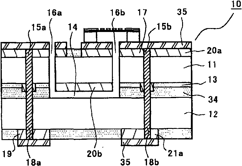
[0042] Refer to the following figure 1 Embodiments of the present invention will be described in detail.

[0043] first, figure 1 A cross-sectional view showing a circuit board having a cavity according to the present invention.

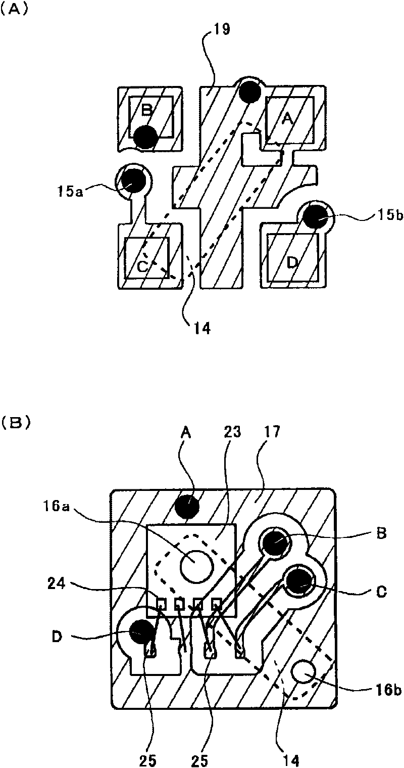
[0044] The circuit board 10 having a cavity includes an upper substrate 11, a lower substrate 12, an adhesive layer 13, a cavity 14, through-hole electrodes 15a, 15b, and through-holes 16a, 16b.

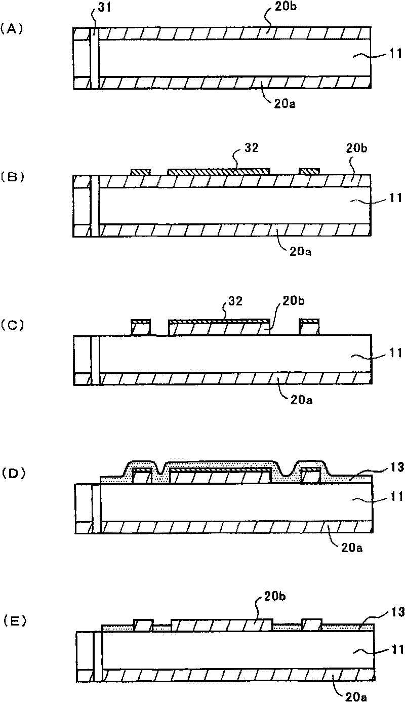
[0045] The upper substrate 11 is a glass epoxy substrate with conductive foils 20a, 20b bonded on both surfaces. The conductive foil 20b having the same shape as the hollow portion is etched at an arbitrary position of the rear conductive foil 20b. The periphery of the hollow-pattern conductive foil 20b is surrounded by a bonding sheet to be the adhesive layer 13 or the like.

[0046] The conductive foil 20a on the surface has a first circuit pattern 17, and the first circuit pattern 17 is formed by exposure, development, and etching.

[0047] The lowe...


PUM


Abstract

A circuit board with hollow space portion and method for manufacturing the same, uses two substrates to constitute a hollow space portion therein. The invention includes: a first circuit pattern 17 formed by the conductive foil 20a on the surface of an upper substrate 11, a bonding layer 13 formed on the back of the upper substrate 11, a second circuit pattern 19 formed by the conductive foil 21a on the surface of an lower substrate 12, a hollow space portion 14 formed by removing the conductive foil 21b on the back of the lower substrate 12, and an insulation layer 34 provided surrounding the hollow space portion 14, wherein the bonding layer 13 on the back of the upper substrate 11 is bonded with the insulation layer 34 on the back of the lower substrate 12, a hollow space portion 14 is surrounded by the upper substrate 11, the lower substrate 12 and the insulation layer 34 between the two substrates.

Description

technical field [0001] The present invention relates to a circuit board having a cavity and a manufacturing method thereof, and more particularly to a circuit board having a cavity using two substrates with a cavity formed therebetween and a manufacturing method thereof. Background technique [0002] Figure 7 Indicates a high-density mounting substrate in which IC chips are embedded in the substrate. [0003] The mounting substrate includes: a first substrate 100 , a second substrate 200 , a third substrate 300 , an IC chip 400 , a conductive connection member 500 and a sealing member 600 . The first substrate 100, the second substrate 200, and the third substrate 300 are printed substrates, and a desired wiring pattern is formed. The first substrate 100 and the second substrate 200 are bonded, and a concave portion having a bottom area and a depth capable of accommodating the IC chip 400 is formed on one outer surface. The IC chip 400 is accommodated in the concave porti...

Claims


Application Information

Patent Timeline
Patent Type & Authority Applications(China)
IPC IPC(8): H01L23/13H01L23/48H01L21/48H01L21/50
CPCH01L2224/48091H01L2224/48195H01L2224/48227H01L2924/1461H01L2924/00014H01L2924/00H05K1/11H05K1/18
Inventor 成田悟郎
Owner ELEMENT DENSHI
Learn More