Micro-nano semiconductor edge emission FP laser and manufacturing method thereof

A laser, edge-emitting technology, used in semiconductor lasers, lasers, laser parts and other directions, can solve problems such as unsatisfactory results, high at 50 microns, and thresholds around 60 mA, achieving high light field output efficiency, Good repeatability and compatibility, overcoming the effect of directional output

Inactive Publication Date: 2010-06-30
INST OF SEMICONDUCTORS - CHINESE ACAD OF SCI
View PDF0 Cites 9 Cited by
  • Summary
  • Abstract
  • Description
  • Claims
  • Application Information

AI Technical Summary

Problems solved by technology

But the current experimental results are not very ideal, such as InP/InGaAsP

Method used


Image

  • Micro-nano semiconductor edge emission FP laser and manufacturing method thereof
  • Micro-nano semiconductor edge emission FP laser and manufacturing method thereof
  • Micro-nano semiconductor edge emission FP laser and manufacturing method thereof

Examples


Embodiment Construction

[0037] In order to make the object, technical solution and advantages of the present invention clearer, the present invention will be described in further detail below in conjunction with specific embodiments and with reference to the accompanying drawings.

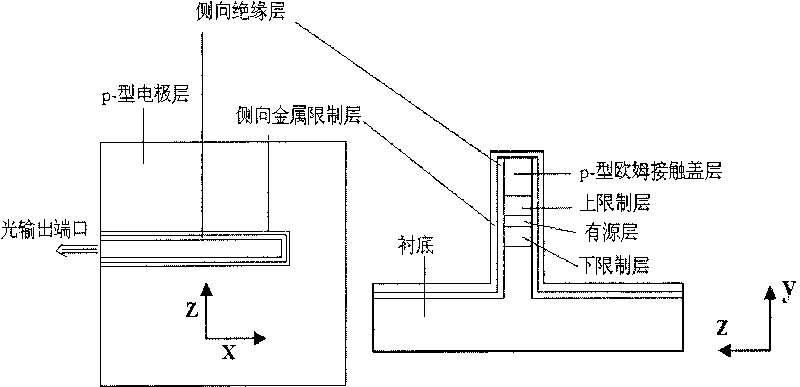
[0038] like figure 1 as shown, figure 1The structure of the micro-nano semiconductor edge-emitting FP laser provided by the present invention, the edge-emitting FP laser includes an n-type substrate 1, a lower confinement layer 2, an active layer 3, an upper confinement layer 4, a P Type ohmic contact cover layer 5, side insulating layer 6 and positive and negative electrode layers 7, wherein the side insulating layer 6 and the P-type electrode layer in the positive and negative electrode layers 7 are used to limit the light field laterally, and enhance the light field on the side of the cavity Or mode confinement, reduce the cavity lasing threshold, improve the exit efficiency of the cavity end face and the output power...


PUM


Abstract

The invention discloses a micro-nano semiconductor edge emission FP laser and manufacturing method thereof. The edge emission FP laser comprises an n-shape underlay (1), a lower limiting layer (2), an active layer (3), an upper limiting layer (4), a P-type ohm contact cap layer (5), a side surface insulating layer (6) and an anode-cathode layer (7) in sequence from up to down; wherein the side surface insulating layer (6) and a P-type electrode layer in the anode-cathode layer (7) are used for laterally limiting a light field, enhancing the lateral light field or the mode limitation of a cavity, reducing the laser emission threshold of the cavity, and improving the exiting efficiency of the end surface of the cavity and the output power of the laser. The invention can be used to overcome the problem of directional output of the micro-nano semiconductor laser, and is easy to analyze the FP mode exited by the laser. A laser source in opto-electronic integration can reach a nano size on a 2D direction and the integration level of opto-electronic apparatuses is improved.

Description

technical field [0001] The invention relates to the technical field of semiconductor optoelectronic devices, in particular to a micro-nano semiconductor edge-emitting FP laser and a manufacturing method thereof. Background technique [0002] A micro-nano laser (microlaser) is a laser composed of a resonant cavity and a gain medium whose size is close to the wavelength of light. With the rapid development of modern communication and integrated optoelectronic technology, micro-nano lasers have broad application prospects as micro-light sources and micro-detectors in the field of optical integration. Due to the advantages of short cavity length, high quality factor, low threshold, and easy optical integration, micro-nano lasers have aroused great interest of many researchers in the past decade. Combined with the existing mature semiconductor plane manufacturing process, its research has made great progress. [0003] In 1992, S.L.McCall et al. of Bell Laboratories in the Unite...

Claims


Application Information

Patent Timeline
IPC IPC(8): H01S5/10H01S5/343H01S5/06
Inventor 车凯军黄永箴
Owner INST OF SEMICONDUCTORS - CHINESE ACAD OF SCI
Why Eureka
Try Eureka