On-chip antenna structure in integrated circuit and manufacturing method thereof

A technology of an on-chip antenna and a manufacturing method, which is applied in the direction of a loop antenna with a ferromagnetic material core, a circuit, and a radiating element structure, etc. Due to the large size of the antenna, the effects of wide process adaptability, reduced size, and increased impedance bandwidth are achieved.

Inactive Publication Date: 2010-07-14
SHANGHAI INTEGRATED CIRCUIT RES & DEV CENT
View PDF8 Cites 7 Cited by
  • Summary
  • Abstract
  • Description
  • Claims
  • Application Information

AI Technical Summary

Problems solved by technology

[0004] The present invention aims to solve the problems in the prior art that the on-chip antenna has a large size, poor transmission performance, performance is easily affected by accessory metal components, and performance is easily affected by the packaging structure.

Method used


Image

  • On-chip antenna structure in integrated circuit and manufacturing method thereof
  • On-chip antenna structure in integrated circuit and manufacturing method thereof
  • On-chip antenna structure in integrated circuit and manufacturing method thereof

Examples


Embodiment Construction

[0038] In order to make the technical features of the present invention more comprehensible, specific embodiments are given below in conjunction with the accompanying drawings to further describe the present invention.

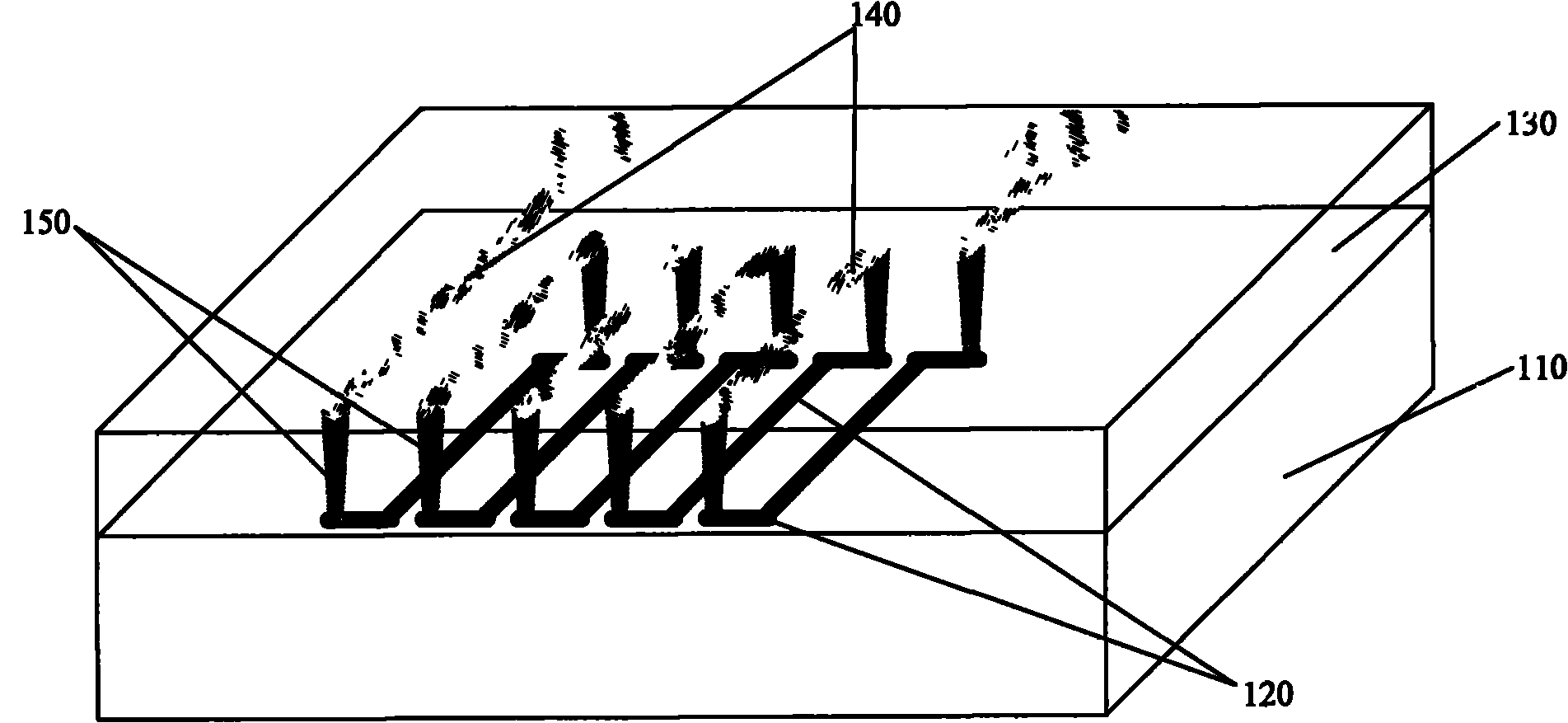
[0039] See figure 1 , shows a schematic structural diagram of an on-chip antenna in an integrated circuit provided by an embodiment of the present invention.

[0040] The on-chip antenna includes: a semiconductor substrate 110; a first metal wire layer 120 disposed on the semiconductor substrate 110; a dielectric layer 130 disposed on the first metal wire layer 120; a second metal wire layer 140 , disposed on the dielectric layer 130 ; an interlayer connection 150 disposed in the dielectric layer 130 to connect the first metal wire layer 120 and the second metal wire layer 140 . The on-chip antenna adopts a double-layer metal interconnection layer combination structure, which not only increases the radiation volume of the on-chip antenna, but also reduces the...


PUM


Abstract

The invention discloses an on-chip antenna structure in an integrated circuit and a manufacturing method thereof. The on-chip antenna structure comprises a semiconductor substrate, a first metal wire layer arranged on the semiconductor substrate, a medium layer arranged on the first metal wire layer, a second metal wire layer arranged on the medium layer, an inter-layer connector arranged in the medium layer for connecting the first metal wire layer and the second metal wire layer. In the structure, a multilayer metal connected layer combined structure is adopted, so the radiation power of an on-chip antenna is increased, the size of the on-chip antenna is reduced, the impedance bandwidth of the on-chip antenna is increased, the transmission gain of the on-chip antenna in wireless internet application is improved obviously, and no extra chip area is occupied.

Description

technical field [0001] The invention relates to the technical field of integrated circuits, in particular to an on-chip antenna in an integrated circuit and a manufacturing method thereof. Background technique [0002] With the continuous development of microelectronics technology, the scale of integrated circuit components increases geometrically as described by Moore's law. Nowadays, the maturity and application of micron and submicron technology make people pay more and more attention to the signal integrity of interconnection, that is, global interconnection transmission delay, interconnection power consumption and interconnection reliability. Based on the above considerations, many scholars have proposed to use wireless interconnection instead of the existing interconnection system, that is, to use a wireless transceiver system with on-chip integrated antennas, regular amplifiers, codecs and other components to realize such things as local interconnection and global int...

Claims


Application Information

Patent Timeline
Patent Type & Authority Applications(China)
IPC IPC(8): H01Q7/06H01Q1/22H01Q1/38H01L21/02
Inventor 储佳
Owner SHANGHAI INTEGRATED CIRCUIT RES & DEV CENT
Why Eureka
Try Eureka