

Polymetal interconnecting layer combined aerial on chip
A combined antenna and interconnection layer technology is applied in the direction of antennas, antenna arrays, independent antenna unit combinations, etc. It can solve the problems of low practicability, occupying chip area, and large communication transmission loss, etc., to achieve wide process adaptability and improve Effects of transmission gain and increased impedance bandwidth
- Summary
- Abstract
- Description
- Claims
- Application Information
AI Technical Summary
Problems solved by technology
Method used
Image

Examples
Embodiment Construction
[0016] The embodiments of the present invention are described in detail below in conjunction with the accompanying drawings: this embodiment is implemented on the premise of the technical solution of the present invention, and detailed implementation methods and specific operating procedures are provided, but the protection scope of the present invention is not limited to the following the described embodiment.
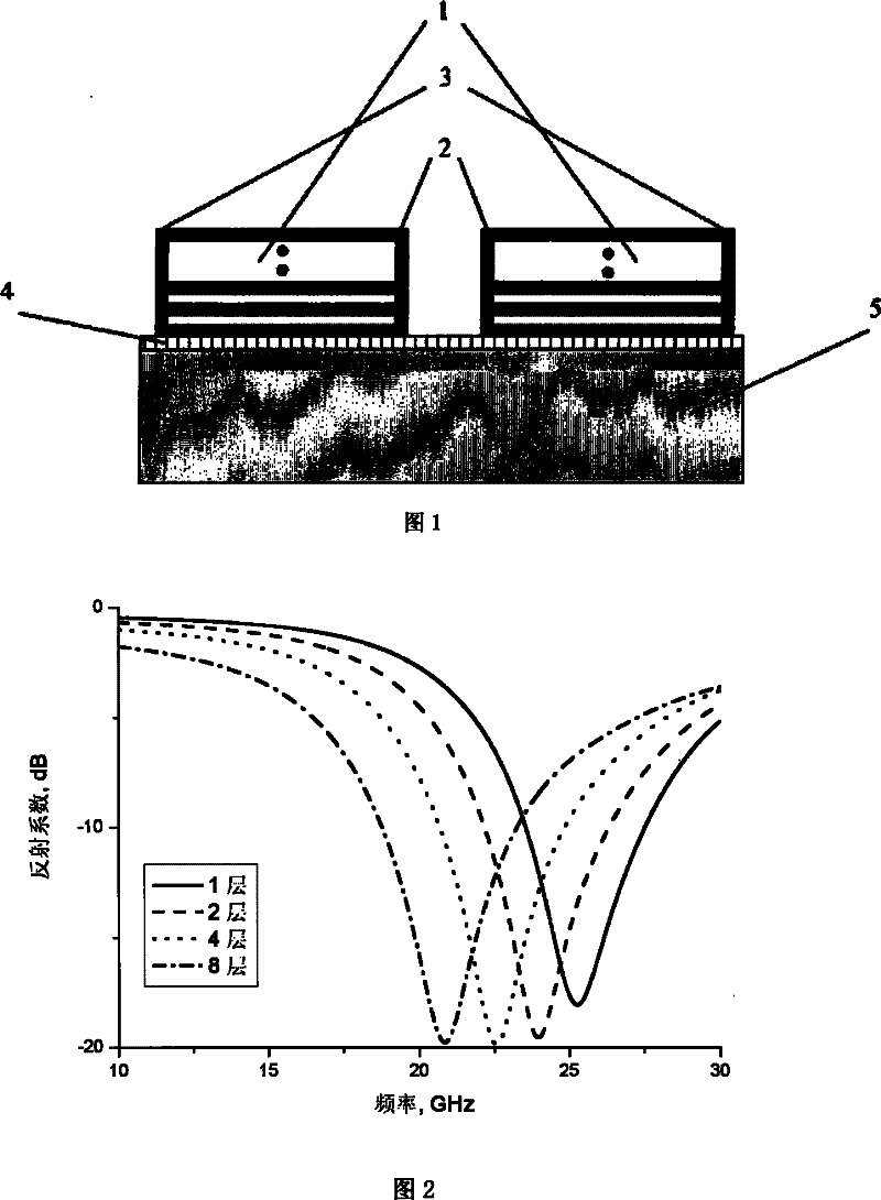
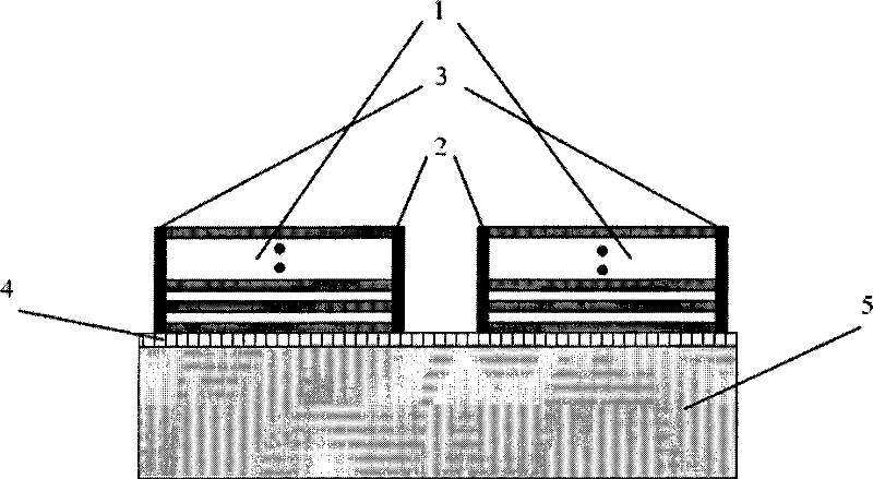
[0017] Such as figure 1 As shown, this embodiment includes: multi-metal interconnection layer radiating element 1 , feed through hole 2 , short circuit through hole 3 , silicon dioxide layer 4 and silicon substrate 5 . The silicon substrate 5 is located at the bottom, the silicon dioxide layer 4 is above it, and the multi-metal interconnection layer radiation element 1 , feed through hole 2 and short circuit through hole 3 are above it. The center of the multi-metal interconnection layer radiating element 1 is connected to the feed through hole 2 , and both ends are ...
PUM
 Abstract
Description
Claims
Application Information