Method for manufacturing capacitor of metal-insulator-metal structure

A manufacturing method and technology for insulators, which are applied in semiconductor/solid-state device manufacturing, semiconductor device, metal material coating process, etc., can solve the problems of reduced performance parameters, high coefficient leakage current, affecting voltage and capacitance curves, etc., to improve performance parameters. Effect

Active Publication Date: 2010-07-21
SEMICON MFG INT (SHANGHAI) CORP +1
View PDF0 Cites 16 Cited by
  • Summary
  • Abstract
  • Description
  • Claims
  • Application Information

AI Technical Summary

Problems solved by technology

[0006] However, due to the inherent instability of the bond itself between the Si-N of SiN generated, the performance parameters of the MIM capacitor with the dielectric layer 102 containing SiN will be reduced, such as will affect the voltage capacitance curve (VCC, Voltage capacitor curve ) coefficient and higher leakage current at high voltage, etc.

Method used


Image

  • Method for manufacturing capacitor of metal-insulator-metal structure
  • Method for manufacturing capacitor of metal-insulator-metal structure
  • Method for manufacturing capacitor of metal-insulator-metal structure

Examples


Embodiment Construction

[0026] In order to make the object, technical solution and advantages of the present invention clearer, the present invention will be further described in detail below with reference to the accompanying drawings and examples.

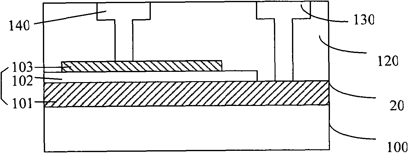
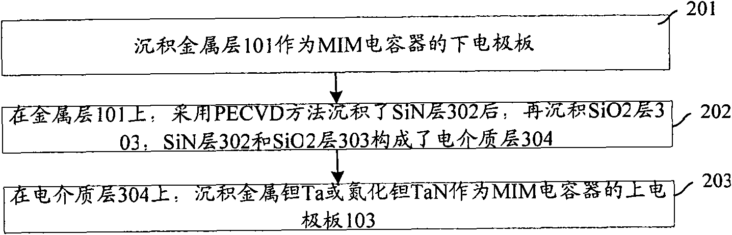
[0027] In order to overcome the performance reduction of the MIM capacitor due to the instability of the bonding bond between Si-N used to manufacture the SiN of the dielectric layer, the present invention deposits a layer of SiO2 at the SiN layer when the dielectric layer is manufactured, the SiO2 The bonding bond between the Si-O layer is more stable than the bonding bond between Si-N, and the SiO2 layer is on the SiN layer, which can cover the SiN layer with low bonding bond stability, which improves the dielectric strength of the manufactured dielectric. Bond stability between atoms in the layer, thereby improving the performance parameters of MIM capacitors with this dielectric layer.

[0028] combine Figure 3a~3c The sectional structure diagram ...


PUM


Abstract

The invention discloses a method for manufacturing a capacitor of a metal-insulator-metal (MIM) structure. The manufacturing method comprises the following steps: firstly, depositing a lower electrode plate; secondly, manufacturing a dielectric layer; and finally, depositing an upper electrode plate. The method for manufacturing the dielectric layer comprises the steps of: depositing a SiO2 layer after depositing a SiN layer. The method provided by the invention has the advantage of improving performance parameters of the MIM capacitor.

Description

technical field [0001] The invention relates to the technical field of semiconductor manufacturing, in particular to a method for manufacturing a metal-insulator-metal capacitor (MIM, Metal-Insulator-Metal). Background technique [0002] Capacitors are widely used in semiconductor integrated circuits as charge storage, coupling and filtering devices. Generally, in order to improve the performance of radio frequency (RF, Radio Frequency) integrated circuits or mixed signal integrated circuits, it is necessary to use large-capacity capacitors. As semiconductor technology enters the 90 nanometer (nm) process node, the feature size of devices in integrated circuits continues to decrease, and high-performance, high-density connections between devices are not only interconnected in a single interconnect layer, but also in multiple layers. interconnection between. Therefore, a large number of connections between devices use a multilayer interconnection structure, in which multipl...

Claims


Application Information

Patent Timeline
Patent Type & Authority Applications(China)
IPC IPC(8): H01L21/02H01L29/92C23C16/34C23C16/40
Inventor 邹晓东徐强邹建军
Owner SEMICON MFG INT (SHANGHAI) CORP
Why Eureka
Try Eureka