Capacitor and inductor scheme with e-fuse application

a technology of capacitors and inductors, applied in the direction of capacitors, semiconductor/solid-state device details, capacitors, etc., can solve the problems of circuit malfunction, large chip area of devices, interference between capacitors/inductors and other parts of the circuit, etc., and achieve the effect of improving parametric performan

Inactive Publication Date: 2008-03-25
TAIWAN SEMICON MFG CO LTD
View PDF11 Cites 14 Cited by
  • Summary
  • Abstract
  • Description
  • Claims
  • Application Information

AI Technical Summary

Benefits of technology

[0012]To achieve these and other objects, and in view of its purposes, an aspect of the invention provides an effective and manufacturable method to form radio frequency (RF) devices in an integrated circuit device. A further object of the invention is to provide a method to form MIM capacitors having improved parametric performance.
[0013]A further object of the invention is to provide a method to form inductors having improved parametric performance. Another object of the invention is to provide a method to form RF devices producing less interference with other circuits in the integrated circuit device. Yet another object of the invention is to provide both capacitors and inductors in a top metal layer.

Problems solved by technology

For integrated circuit devices, the formation of large value capacitors and inductors presents a unique challenge for several reasons.
First, these devices can consume large chip areas.
Second, there can be interference between the capacitor / inductor and other parts of the circuit.
These interactions can cause circuit malfunctions and tend to reduce the linearity of the RF devices.
Third, it can be difficult to create devices with a large Q value.
Fourth, obtaining precise values is difficult due to process variation.
However, this approach suffers several problems.
Second, the capacitor value is limited by area constraints.
Third, there is a significant risk of interference with other circuit signals since the capacitor is formed in the interconnect routing levels M5 and M6.
Second, the inductor value is limited by the available surface area.
Fourth, the methods of forming the exemplary spiral inductor and capacitor are not compatible.

Method used


Image

  • Capacitor and inductor scheme with e-fuse application
  • Capacitor and inductor scheme with e-fuse application
  • Capacitor and inductor scheme with e-fuse application

Examples


first embodiment

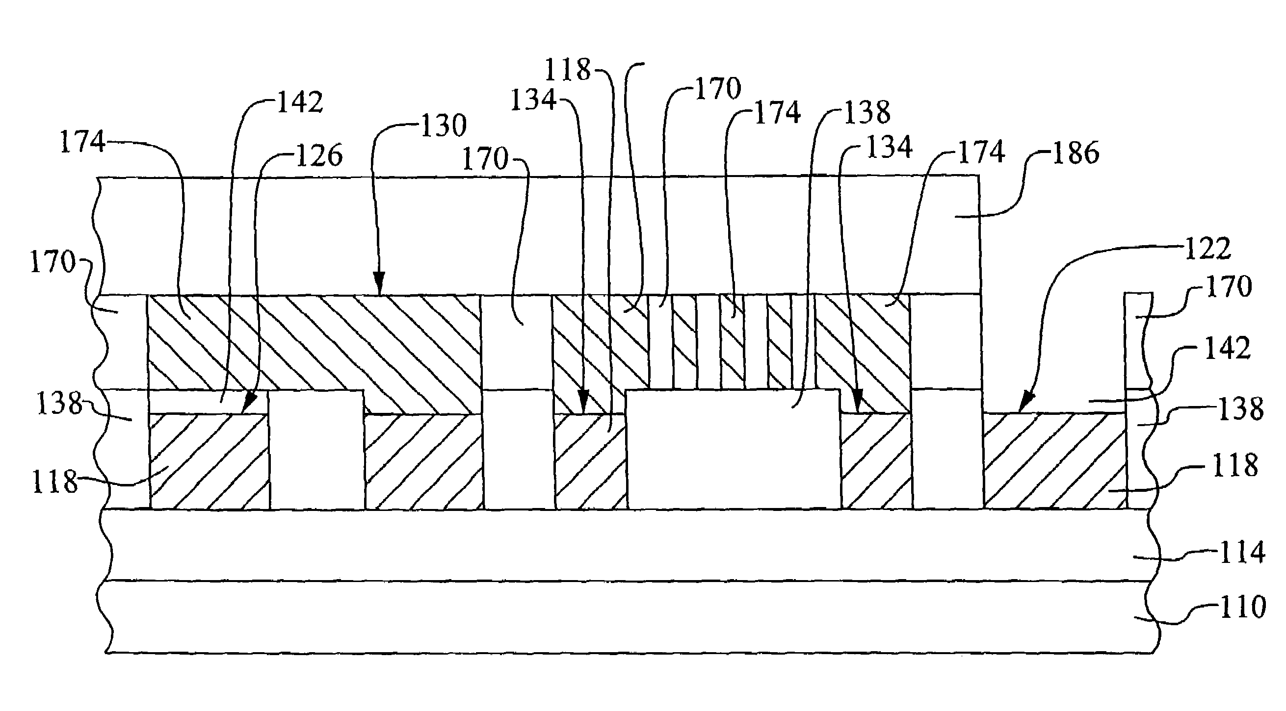
[0032]In the first embodiment, the top metal level 118 is defined using a deposit / etch process. In this embodiment, the top metal level 118 is deposited overlying the insulating layer 114. The top metal level 118 may be deposited using, for example, physical vapor deposition (PVD) or sputtering. Further, the top metal level 118 may comprise aluminum, copper, or an alloy of aluminum and copper. Further, the top metal level 118 may comprise a series of layers. For example, a barrier layer such as titanium nitride may be formed over or under an aluminum / copper layer to create the entire top metal level 118.

[0033]Referring now to FIG. 6, as an important step in a deposit / etch sequence, the deposited top metal level 118 is patterned. For example, a photoresist layer, not shown, may be coated overlying the metal level 118. The photoresist layer is then exposed to actinic light through a mask and developed. The remaining photoresist layer is then used to mask the metal level 118 during a m...

second embodiment

[0043]Referring now to FIGS. 12 through 14, the invention is illustrated. In this case, a damascene process may be used to define the top metal level and the RF metal level. If copper is used for the metal levels, then it may be necessary to use a damascene process technique to define these metal level since it is very difficult to precisely etch copper.

[0044]In this second exemplary embodiment, the step of defining the top metal level 118 comprises, first, depositing the top level dielectric 138 overlying the substrate 110. The top level dielectric 138 may comprise a first passivation layer. The top level dielectric 138 is patterned to form trenches. The top metal level 118 is deposited overlying the top level dielectric 138 and filling the trenches. The top metal level 118 is then planarized. This planarization may comprise, for example, a chemical mechanical polish (CMP) step where the metal is polished down to below the top level dielectric layer 138. Other planarization approac...


PUM


Abstract

RF devices formed in integrated circuit devices include a top metal level overlying a substrate. The top metal level comprises pads and portions of planned RF devices and an RF metal level overlying the top metal level completes the RF devices which may be an interconnected RF network that may include capacitors, inductors or both. Openings are formed in a passivation layer overlying the RF metal level to provide direct access to the RF devices. The interconnected RF network may include fuses enabling the network to be selectively altered by cutting relatively thin interconnect lines using a laser directed through the openings. The RF devices or portions of the RF network may be directly coupled to external devices and utilized in SOC (System On a Chip) and SIT (System In Package) technologies.

Description

RELATED APPLICATIONS[0001]This application is a Continuation-in-part of application Ser. No. 10 / 926,836 filed Aug. 26, 2004, now U.S. Pat. No. 7,183,625, which is a Divisional Application of application Ser. No. 10 / 314,664, filed Dec. 9, 2002 and now issued as U.S. Pat. No. 6,800,534, the contents of each of which are hereby incorporated in their entireties by reference.FIELD OF THE INVENTION[0002]The invention relates to a structure and method for RF devices in an integrated circuit device, and, more particularly, to an alterable network of RF devices at a chip top level and individually accessible by remote components.BACKGROUND OF THE INVENTION[0003]Many types of electronic circuits require relatively large value capacitors and inductors. In particular, radio frequency (RF) circuits are those that function at high frequency levels even above the microwave range. Capacitors and inductors are passive components and are herein called RF devices. These RF devices frequently appear in...

Claims


Application Information

Patent Timeline
Patent Type & Authority Patents(United States)
IPC IPC(8): H01L29/00H01L21/02H01L23/522H01L27/08
CPCH01L23/5223H01L23/5227H01L27/08H01L28/10H01L28/40H01L2924/0002H01L2924/00
Inventor HSIEH, YEOU-LANGHUANG, CHING-KWUNCHU, YI-JING
Owner TAIWAN SEMICON MFG CO LTD
Why Eureka
Try Eureka