Semiconductor device

A semiconductor, top-side technology, applied in the direction of semiconductor devices, semiconductor/solid-state device manufacturing, semiconductor/solid-state device components, etc., can solve the problem of reducing the degree of freedom of the side wiring position, to improve the positional freedom, reduce the chip area, easy-to-create effects

Active Publication Date: 2012-04-11
MITSUBISHI ELECTRIC CORP
View PDF1 Cites 0 Cited by
  • Summary
  • Abstract
  • Description
  • Claims
  • Application Information

AI Technical Summary

Problems solved by technology

Therefore, once the position of the side wiring is changed, the side wiring is not connected to the top wiring, thus reducing the degree of freedom in the position of the side wiring

Method used


Image

  • Semiconductor device
  • Semiconductor device
  • Semiconductor device

Examples


Embodiment approach 1

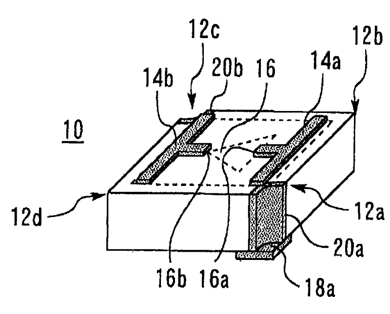
[0021] figure 1 , figure 2 It is a perspective view showing the semiconductor chip of Embodiment 1. The semiconductor chip 10 has top and bottom surfaces facing each other and side surfaces connecting the top and bottom surfaces. The top surface of the semiconductor chip 10 has a corner 12a, a corner 12b adjacent to the corner 12a, a corner 12c existing on the diagonal of the corner 12a, and a corner existing on the diagonal of the corner 12b. The quadrilateral of part 12d.

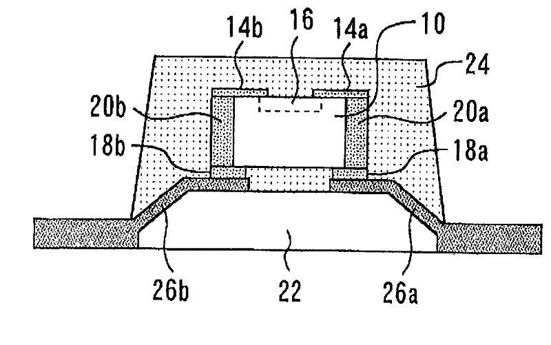
[0022] On the top surface of the semiconductor chip 10, a top wiring 14a is formed to connect the corner 12a and the corner 12b, and a top wiring 14b is formed to connect the corner 12c and the corner 12d. Electronic circuitry 16 is formed on the top surface of semiconductor chip 10 . The electronic circuit 16 has an input terminal 16b connected to the top wiring 14a and an output terminal 16a connected to the top wiring 14b. Bottom electrode 18a is formed at a corner of the bottom surface correspon...

Embodiment approach 2

[0037] Figure 7 It is a perspective view showing the semiconductor chip of Embodiment 2. The semiconductor chip 10 has top and bottom surfaces facing each other and side surfaces connecting the top and bottom surfaces. The top surface of the semiconductor chip 10 is quadrangular.

[0038] On the top surface of the semiconductor chip 10 , top surface wiring 14 is formed along the outer periphery of the top surface. Electronic circuitry 16 is formed on the top surface of semiconductor chip 10 . The electronic circuit 16 has an input terminal 16 b connected to the top surface wiring 14 and an output terminal 16 a connected to the lead pad 36 . A bottom electrode 18 is formed on the bottom surface of the semiconductor chip 10 .

[0039] A side wiring 20 is formed on a side surface of the semiconductor chip 10 . The side wiring 20 connects the top wiring 14 and the bottom electrode 18 . The input terminal 16 b of the electronic circuit 16 is connected to the side wiring 20 v...


PUM


Abstract

The invention can obtain a semiconductor device that can be easily produced and can reduce the chip area. The semiconductor chip has a top surface, a bottom surface and a lateral surface connecting the top surface and the bottom surface. Bottom surface electrodes are formed on the bottom surface of the semiconductor chip. Lateral surface wiring is formed on the lateral surface of the corner of the semiconductor chip. The lateral surface wiring is connected to the electronic circuit and the bottom surface electrodes.

Description

technical field [0001] The present invention relates to a semiconductor device in which side wiring is formed on a side surface of a semiconductor chip, and more particularly to a semiconductor device which can be easily manufactured and has a reduced chip area. Background technique [0002] In a semiconductor device in which a semiconductor chip is mounted on a mounting portion, wire bonding, flip chip, side wiring, etc. are used to connect an electronic circuit of the semiconductor chip to electrodes of the mounting portion. Side wiring is formed on the side surface of the semiconductor chip by cutting through holes provided on dicing lines of the semiconductor wafer (for example, refer to Patent Document 1: Japanese Patent Application Laid-Open No. 6-120294). [0003] Conventionally, side wiring is formed on the side of a semiconductor chip. Therefore, side wirings of two semiconductor chips are formed by one through hole. Therefore, many through holes must be formed in...

Claims


Application Information

Patent Timeline
Patent Type & Authority Patents(China)
IPC IPC(8): H01L23/52H01L23/482H01L23/48H01L21/60
CPCH01L2924/0002
Inventor 细见刚石田多华生相原育贵宫胁胜巳
Owner MITSUBISHI ELECTRIC CORP
Why Eureka
Try Eureka