High-density low-parasitic capacitor

A capacitive device, low parasitic technology, applied in the direction of circuits, electrical components, electric solid-state devices, etc., can solve problems that affect circuit performance and limit applications, and achieve the effect of improving performance, reducing additional power consumption, and achieving remarkable results

Active Publication Date: 2010-07-28
INST OF SEMICONDUCTORS - CHINESE ACAD OF SCI
View PDF4 Cites 6 Cited by
  • Summary
  • Abstract
  • Description
  • Claims
  • Application Information

AI Technical Summary

Problems solved by technology

For capacitors implemented by NMOS tubes, one end of the capacitor must be grounded, which limits its application
For the capacitance realized by PMOS transistor, due to the large parasitic capacitance between the N well and the P substrate, the parasitic capacitance is usually about 10% to 20% of the effective capacitance, which will cause additional power consumption in the circuit and affect the circuit. performance

Method used


Image

  • High-density low-parasitic capacitor
  • High-density low-parasitic capacitor
  • High-density low-parasitic capacitor

Examples


Embodiment Construction

[0027] In order to make the object, technical solution and advantages of the present invention clearer, the present invention will be described in further detail below in conjunction with specific embodiments and with reference to the accompanying drawings.

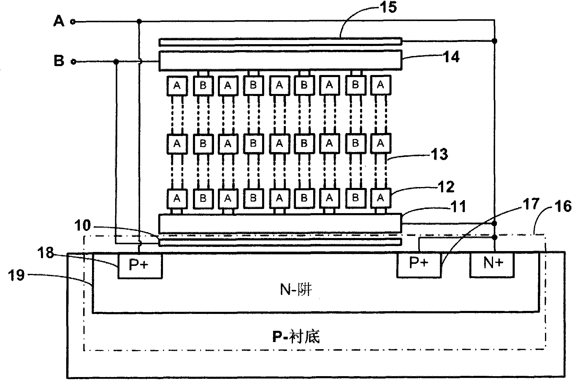
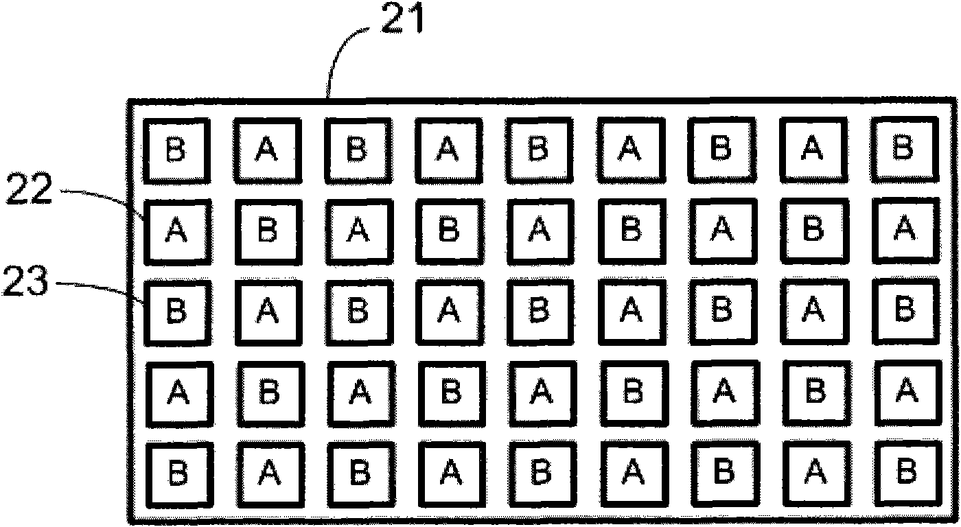
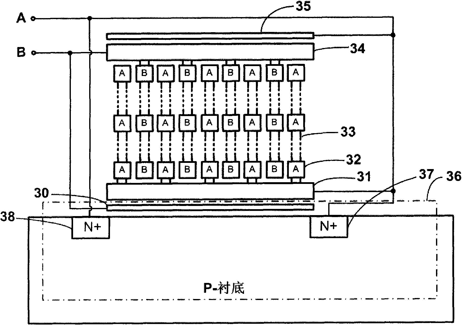
[0028] This high-density and low-parasitic capacitance device proposed by the present invention firstly realizes the maximization of capacitance per unit area, and secondly can effectively reduce the parasitic capacitance from the N well to the P substrate in the PMOS capacitance. In addition, the present invention adopts The special interlayer metal interconnection structure can maximize the capacitance between the same metal layers and the capacitance between via holes. With the decrease of process feature size, the improvement of lithography accuracy and the increase of metal layers, The distance between the metal layer and the metal layer, and the through hole can be further reduced, and the effective capacitance can b...


PUM


Abstract

The invention discloses a high-density low-parasitic capacitor, comprising a PMOS capacitor, a first capacitor, a second capacitor, a third capacitor and an MIM capacitor, wherein the PMOS capacitor is composed of a polysilicon gate, gate oxide, and a source electrode, a drain electrode and an N-well; the source electrode, the drain electrode and an N-well are connected together; the first capacitor is arranged between the polysilicon gate and the metal at the first layer; the second capacitor is arranged between metals at the same layer; the metal at the first layer is composed of a metal block array, and each metal block and an adjacent metal block thereof are respectively connected with the port A and port B of the second capacitor; the third capacitor is arranged between through holes, and each through hole and an adjacent through hole thereof are respectively connected with the port A and port B of the capacitor; and the MIM capacitor is provided an upper polar plate and a lower polar plate which are respectively connected to the port A and port B of the capacitor. In the invention, the capacitor between the polysilicon gate and the metal layer, the capacitor between the metals at the same layer, the capacitor between the through holes, the MIM capacitor and the like are realized on an MOS capacitor, thus reaching the maximal capacitance on a unit area.

Description

technical field [0001] The invention relates to the technical field of integrated circuits, in particular to a high-density and low-parasitic capacitance device, which can be applied to multiple sub-fields under integrated circuits, such as memory, RFID, charge pump and the like. Background technique [0002] How to maximize the use of integrated circuit technology to manufacture high-density, low parasitic, and high-precision capacitors is crucial to various fields of integrated circuit design. High-density capacitors can greatly reduce the chip area and cost; and low parasitic capacitors can reduce the extra power consumption of the chip; high-precision capacitors can greatly improve the performance of the chip; and high-performance compatible with MOS technology The capacitor can greatly reduce the additional manufacturing cost brought by the chip. [0003] At present, capacitors compatible with the MOS process mainly include MOS capacitors, MIM capacitors, and capacitor...

Claims


Application Information

Patent Timeline
Patent Type & Authority Applications(China)
IPC IPC(8): H01L27/08H01L29/94H01L29/92
Inventor 冯鹏吴南健
Owner INST OF SEMICONDUCTORS - CHINESE ACAD OF SCI
Why Eureka
Try Eureka