Metal oxide semiconductor (MOS) transistor and formation method thereof

A MOS transistor and semiconductor technology, applied in semiconductor devices, semiconductor/solid-state device manufacturing, electrical components, etc., can solve the problems that cannot be further reduced, and achieve the effect of reducing influence and weakening junction capacitance

Inactive Publication Date: 2010-07-28
SEMICON MFG INT (SHANGHAI) CORP
View PDF0 Cites 58 Cited by
  • Summary
  • Abstract
  • Description
  • Claims
  • Application Information

AI Technical Summary

Problems solved by technology

[0008] The problem solved by the present invention is that the existing transistor formation method cannot further reduce the influence of the junction capacitance formed between the source and drain regions and the isolation well, which affects the performance of the transistor device circuit

Method used


Image

  • Metal oxide semiconductor (MOS) transistor and formation method thereof
  • Metal oxide semiconductor (MOS) transistor and formation method thereof
  • Metal oxide semiconductor (MOS) transistor and formation method thereof

Examples


Embodiment Construction

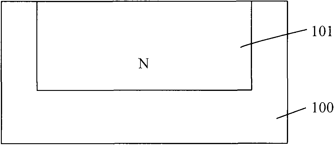
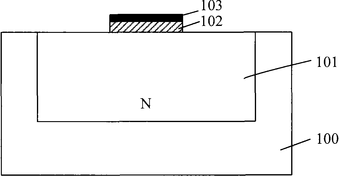
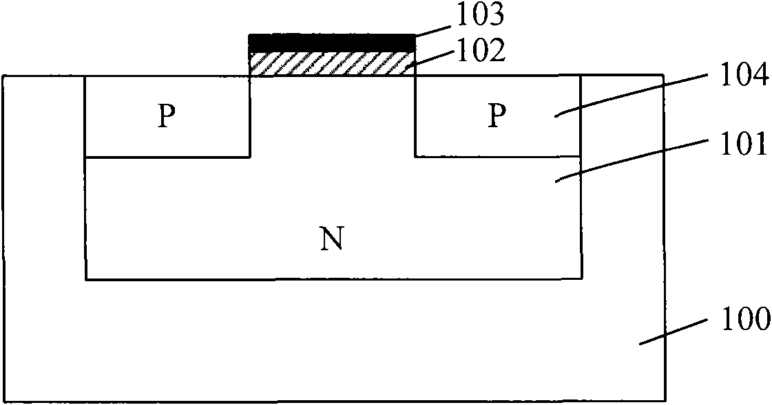
[0031] It is known from the background technology that in the manufacturing process of MOS transistors, the doping concentration near the interface between the isolation well and the source and drain regions determines the size of the junction capacitance in the MOS transistor, so reduce the doping concentration there as much as possible Can effectively eliminate junction capacitance. The doping concentration here can be reduced by performing anti-phase doping on the isolation well to neutralize the two opposite doping substances.

[0032] The invention provides a method for forming a MOS transistor, the process of which is as follows: Figure 5 As shown, the specific implementation is as follows:

[0033] S1, first forming an isolation well on the semiconductor substrate by multiple ion implantation;

[0034] S2. Perform reverse-phase ion implantation on the isolation well;

[0035] Among them, if a PMOS is formed, the isolation well is an N well, and the dopant used in th...


PUM


Abstract

The invention provides a metal oxide semiconductor (MOS) transistor and a formation method thereof. The formation method of the transistor comprises the following steps of: forming an isolated well on a semiconductor substrate through repeated ion injection; carrying out reversed-phase ion injection on the isolated well; and forming a grid electrode, a source region and a drain region of the MOS transistor on the isolated well. The invention reduces the doping concentration nearby the interface of the source and the drain regions and the isolated well so as to weaken the junction capacitance and further reduce the influence of the parasitic junction capacitance on transistor devices, and also keeps the doping concentration on the surface of the isolated well and nearby the interface of the isolated well and the substrate so as to avoid affecting the original properties of the transistor device.

Description

technical field [0001] The invention relates to a MOS transistor, in particular to a MOS transistor subjected to reverse-phase ion implantation and a forming method thereof. Background technique [0002] As the most basic device in semiconductor manufacturing, MOS transistors are widely used in various integrated circuits. According to the main carrier and the doping type during manufacturing, they are divided into PMOS and NMOS. Such as Figure 1 to Figure 3 Shown is the main formation process of a typical PMOS. [0003] first as figure 1 , forming an N well 101 on the semiconductor substrate 100 by ion implantation; [0004] Then if figure 2 , forming an oxide layer 102 and a polysilicon layer 103 on the surface of the N well 101, and etching a part as a gate; [0005] Finally as image 3 , forming a P-type region 104 in the N well 101 on both sides of the gate, respectively serving as the source region and the drain region of the PMOS. [0006] In practical applic...

Claims


Application Information

Patent Timeline
Patent Type & Authority Applications(China)
IPC IPC(8): H01L29/78H01L21/336H01L21/265
Inventor 施雪捷
Owner SEMICON MFG INT (SHANGHAI) CORP
Why Eureka
Try Eureka