Method for processing wafer

A processing method and technology for wafers, which are applied in metal processing equipment, manufacturing tools, machine tools suitable for grinding workpiece planes, etc., can solve problems such as easy breakage of wafers

Inactive Publication Date: 2010-08-18
DISCO CORP
View PDF8 Cites 10 Cited by
  • Summary
  • Abstract
  • Description
  • Claims
  • Application Information

AI Technical Summary

Problems solved by technology

[0008] However, the wafer from which the ring-shaped reinforcing portion is removed has a problem that it is easily broken during cutting.
Therefore, when dividing a wafer having a ring-shaped reinforcement portion formed on the outer periphery of the back surface into individual devices, there is a problem of when to remove the ring-shaped reinforcement portion.

Method used


Image

  • Method for processing wafer
  • Method for processing wafer
  • Method for processing wafer

Examples


Embodiment Construction

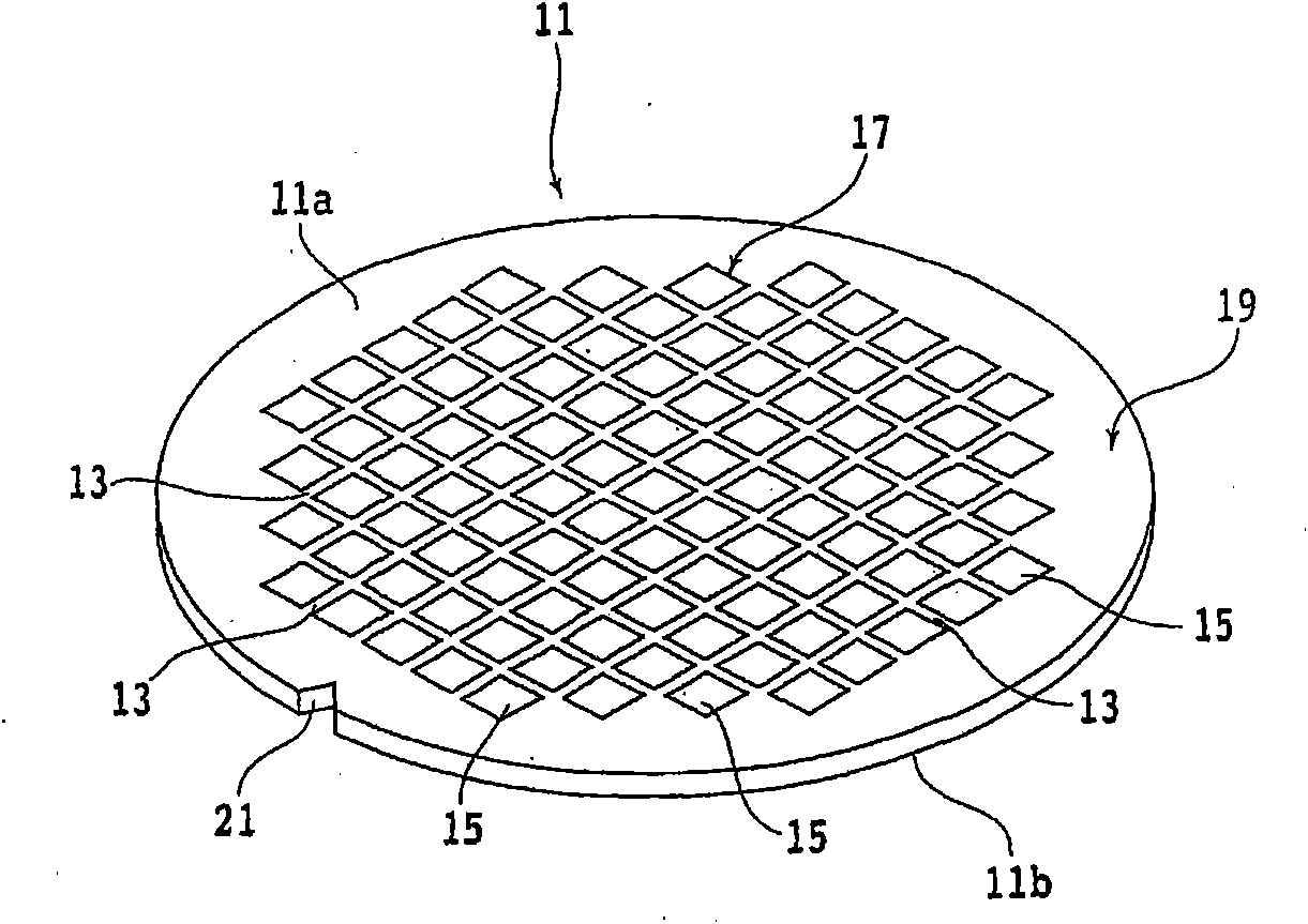
[0026] Hereinafter, embodiments of the present invention will be described in detail with reference to the drawings. figure 1 It is a perspective view of a semiconductor wafer before processing to a predetermined thickness. figure 1 The shown semiconductor wafer 11 is made of, for example, a silicon wafer with a thickness of 700 μm, and a plurality of partitions 13 are formed in a grid pattern on the surface 11 a, and ICs are formed in a plurality of regions divided by the plurality of partitions 13 . , LSI and other devices 15.

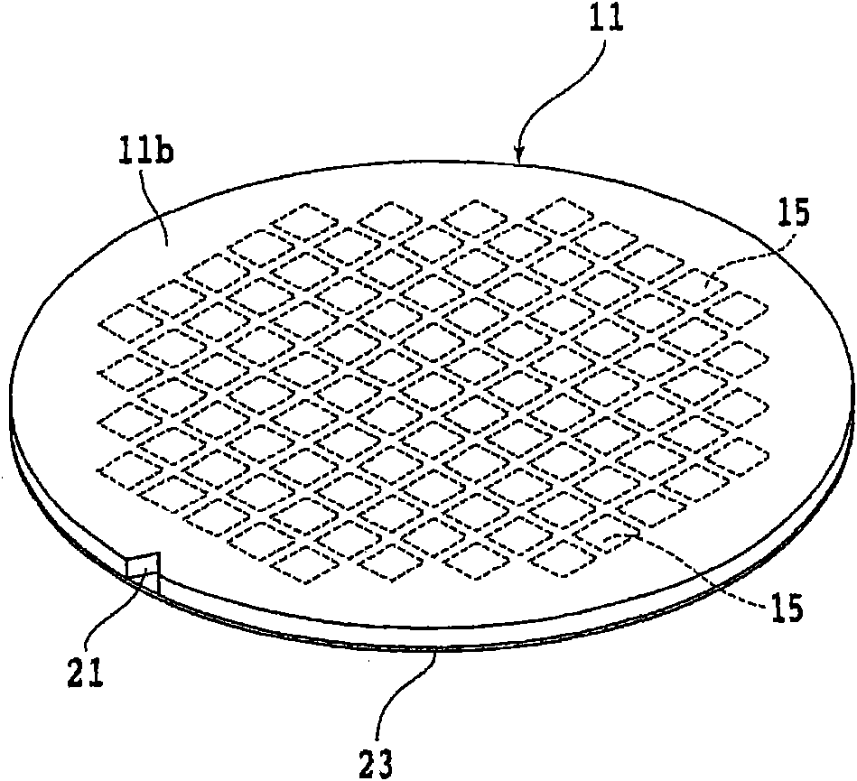
[0027] The semiconductor wafer 11 thus constituted has a device region 17 in which the device 15 is formed, and a peripheral remaining region 19 surrounding the device region 17 . Further, on the outer periphery of the semiconductor wafer 11, a notch 21 is formed as a mark indicating the crystal orientation of the silicon wafer.

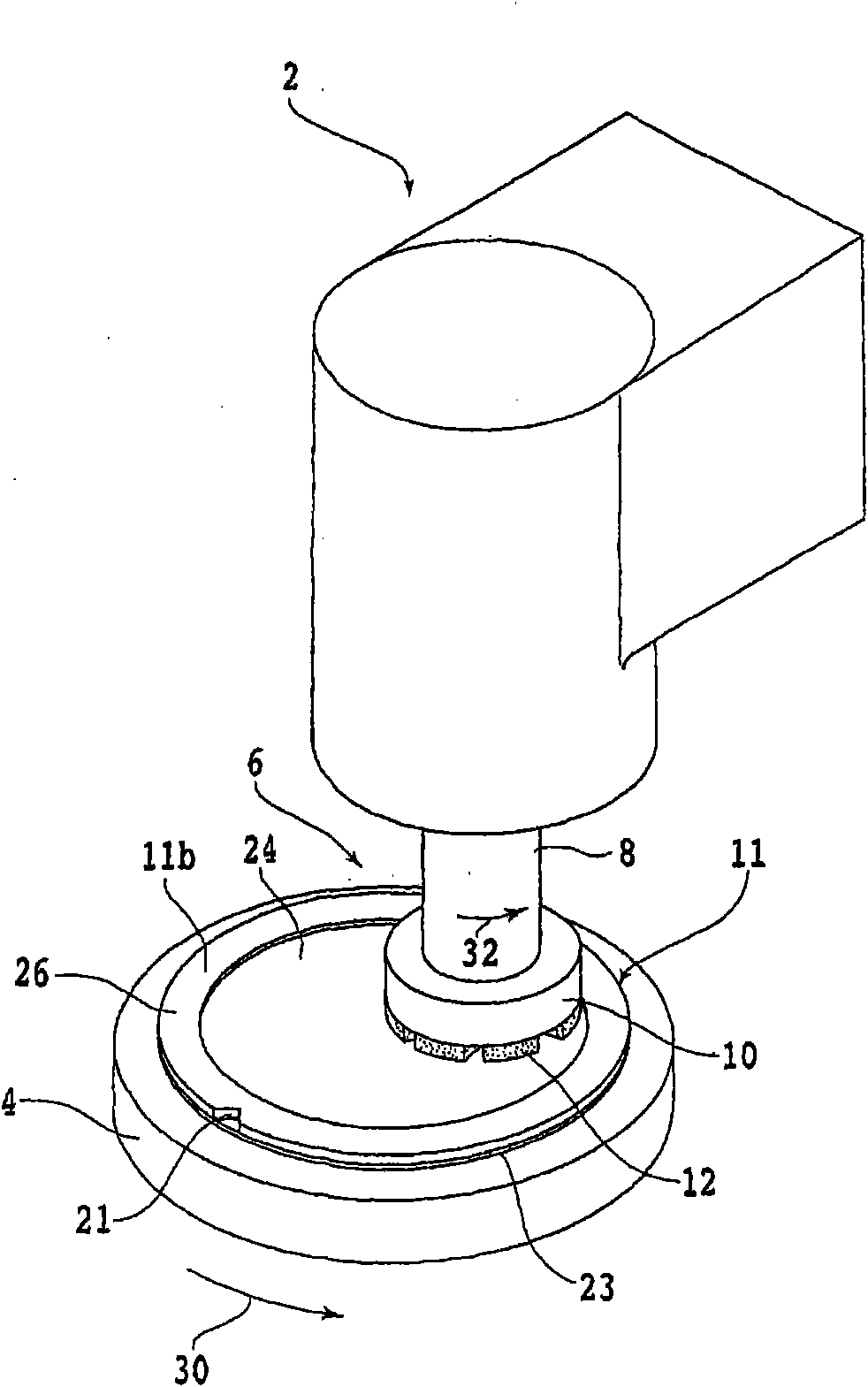
[0028] On the surface 11a of the semiconductor wafer 11, the protective tape 23 is pasted in a protective tape pasting ...


PUM


Abstract

The invention provides a method for processing a wafer, capable of dividing the wafer into a plurality of devices. The wafer has a device area and a peripheral residual area on the surface, the method for processing the wafer includes: a step of grinding the wafer for grinding the back side of the wafer corresponding to the device area to a predetermined thickness to form a ring-shaped enhancing part at the back side corresponding to the peripheral residual area, a step of supporting the wafer for bonding a cutting belt on the back side of the wafer and bonding the peripheral part of the cutting belt on a cutting frame so as to support the wafer by the cutting frame, a step of dividing the wafer for holding the wafer on a chuck workbench locating a cutting tool at the predetermined dividing line and cutting the predetermined dividing line so as to divide the wafer into a plurality of devices, a step of removing the ring-shaped enhancing part for rotating the chuck workbench when the cutting tool is located at the boundary of the device area and the peripheral residual area and cutting off the ring-shaped enhancing part, and a picking step for picking up the plurality of devices from the cutting belt.

Description

technical field [0001] The present invention relates to a wafer processing method capable of dividing a thinly ground wafer into individual devices without impairing handleability. Background technique [0002] In the manufacturing process of a semiconductor device, a plurality of regions are divided on the surface of a substantially disk-shaped semiconductor wafer by dividing lines called streets arranged in a grid pattern, and ICs (Integrated ICs) are formed in the divided regions. Circuit: integrated circuit), LSI (Large Scale Integration: large scale integrated circuit) and other devices. Then, the semiconductor wafer is divided into individual semiconductor chips (devices) by cutting the semiconductor wafer along the lanes with a cutting device. [0003] The divided wafers are formed to a predetermined thickness by grinding the back side before being cut along the lanes. In recent years, in order to achieve weight reduction and miniaturization of electrical equipment,...

Claims


Application Information

Patent Timeline
Patent Type & Authority Applications(China)
IPC IPC(8): H01L21/78H01L21/304
CPCH01L21/3043H01L21/78B24B7/228
Inventor 香西宏彦保罗·文森特·埃藤迪多近藤安昙梶山启一
Owner DISCO CORP
Why Eureka
Try Eureka