Silicon slice alignment method for silicon through hole interconnection

A technology of silicon wafer alignment and through-silicon vias, which is applied in the manufacture of electrical components, electrical solid-state devices, semiconductor/solid-state devices, etc., can solve the problems affecting the working frequency of chips and the interconnection resistance of silicon wafers, and achieve low power consumption , high-speed power consumption, and the effect of reducing interconnect resistance

Inactive Publication Date: 2010-08-25
FUDAN UNIV
View PDF2 Cites 7 Cited by
  • Summary
  • Abstract
  • Description
  • Claims
  • Application Information

AI Technical Summary

Problems solved by technology

When stacking, the alignment of the silicon wafers will affect the interconnection resistance between the silicon wafers, which in turn affects the operating frequency of the chips, so that the three-dimensional stacking of chips cannot be applied in a wider field

Method used


Image

  • Silicon slice alignment method for silicon through hole interconnection
  • Silicon slice alignment method for silicon through hole interconnection
  • Silicon slice alignment method for silicon through hole interconnection

Examples


Embodiment Construction

[0016] An exemplary embodiment of the present invention will be described in detail below with reference to the accompanying drawings. The reference figure is a schematic diagram of an idealized embodiment of the present invention, and the following embodiments are only illustrative, and the present invention is not limited by the following embodiments.

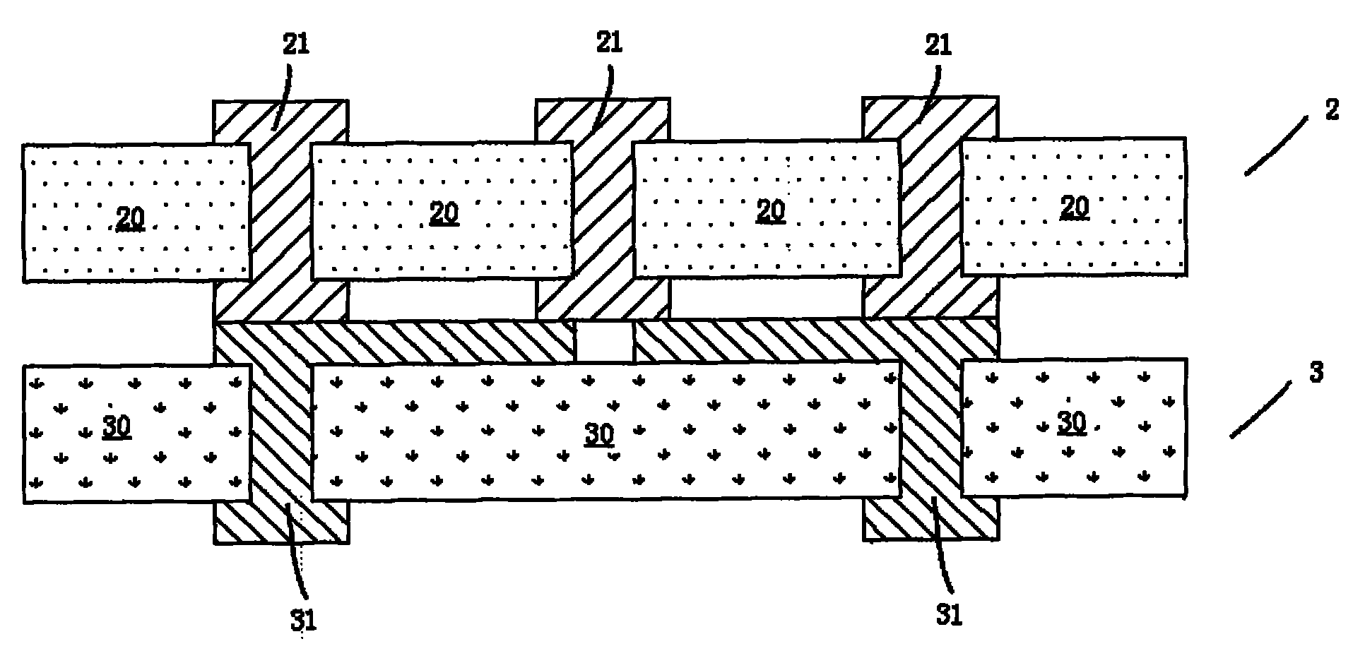
[0017] Provide two silicon wafers with TSV structures and interconnection solder joints completed, and FIG. 1 is a side view of the provided silicon wafers. As shown in Figure 1, in the silicon wafer 2, 20 is the silicon part, 21 is the through-silicon hole and the interconnection pad; in the silicon wafer 3, the 30 is the silicon part, and the 31 is the through-silicon hole. holes and interconnect solder joints.

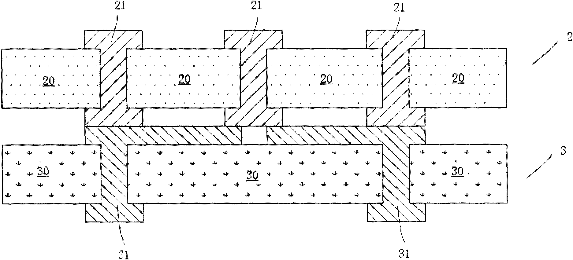
[0018] Next, silicon wafer 2 and silicon wafer 3 are stacked and interconnected, as shown in FIG. 2 .

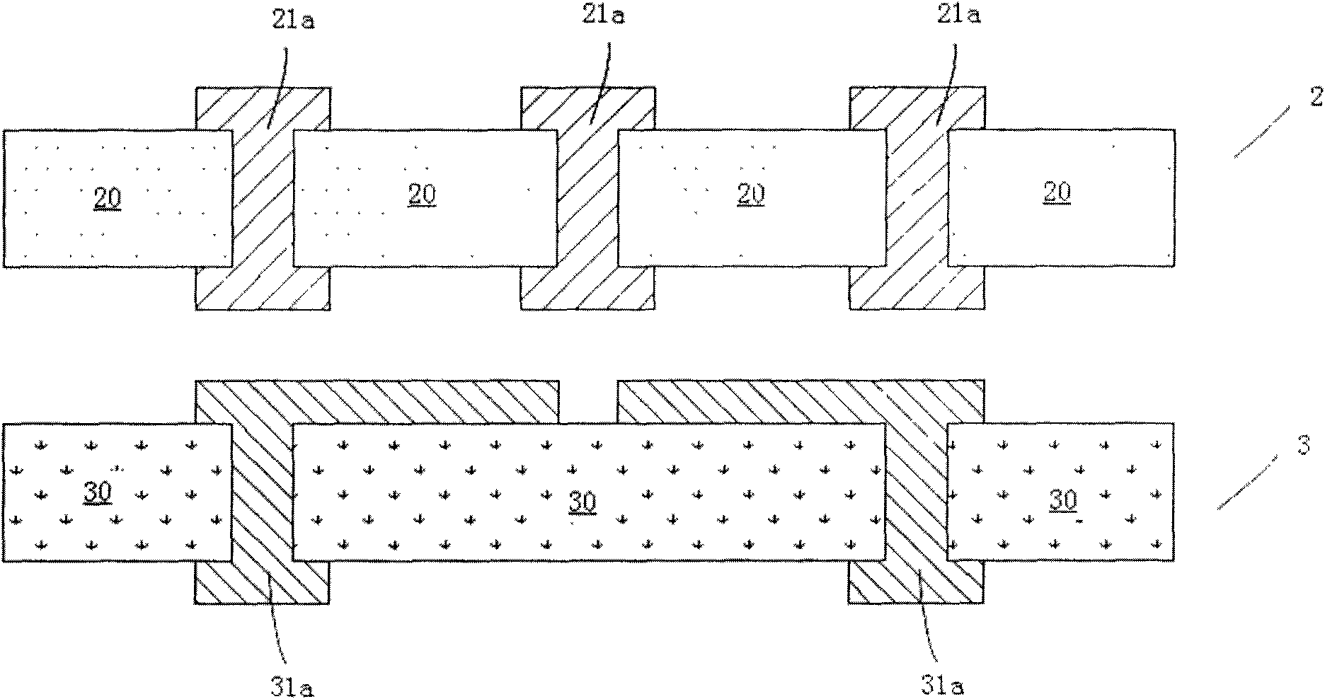
[0019] When the silicon wafer 2 and the silicon wafer 3 are in contact, there may be misalignment between th...


PUM


Abstract

The invention belongs to the technical field of high-integration encapsulation, and particularly discloses a silicon slice alignment method for silicon through hole interconnection. The method comprises that: stacked and interconnected upper and lower silicon slices are aligned and corrected by adopting an electric method when a plurality of silicon slices are stacked and interconnected, so the alignment precision of the silicon slices can be improved and the interconnected resistance can be reduced. The integrated circuit chip manufactured by the method has the performance of high speed and low power consumption.

Description

technical field [0001] The invention belongs to the technical field of high-integration packaging, and in particular relates to a through-silicon via interconnect packaging method. Background technique [0002] With the continuous development of microelectronics technology, the miniaturization of chip manufacturing technology has promoted the continuous development of integrated circuit packaging technology, and gradually formed a relatively independent technology industry. Now, three-dimensional packaging technology has been considered as the development trend of integrated circuit packaging in the future, and three-dimensional packaging technology has developed from chip-level stacked die or package on package technology to wafer-level silicon Through-hole (Through Silicon Via, TSV) interconnect packaging technology. [0003] Through silicon via interconnection technology is to make vertical through holes between silicon wafers, and then form interconnection micro solder ...

Claims


Application Information

Patent Timeline
Patent Type & Authority Applications(China)
IPC IPC(8): H01L21/68H01L21/50H01L21/60
CPCH01L2225/06593H01L2924/0002H01L25/50H01L2225/06513H01L2225/06541H01L25/0657H01L23/481H01L2224/16
Inventor 王鹏飞孙清清丁士进张卫
Owner FUDAN UNIV
Why Eureka
Try Eureka