Power device and method for performing conductivity modulation by using photoelectron injection

A power device, conductance modulation technology, applied in semiconductor devices, electrical components, circuits, etc., can solve the problems of complex super junction technology, high production cost, high device parameter requirements, etc., to reduce the characteristic on-resistance and improve performance. , the effect of reducing the doping concentration

Inactive Publication Date: 2010-08-25
FUDAN UNIV
View PDF2 Cites 14 Cited by
  • Summary
  • Abstract
  • Description
  • Claims
  • Application Information

AI Technical Summary

Problems solved by technology

However, the process of super junction technology is complicated, and at the same time, the parameters of the device are very high, and the production cost is relatively high.

Method used


Image

  • Power device and method for performing conductivity modulation by using photoelectron injection
  • Power device and method for performing conductivity modulation by using photoelectron injection
  • Power device and method for performing conductivity modulation by using photoelectron injection

Examples


Embodiment Construction

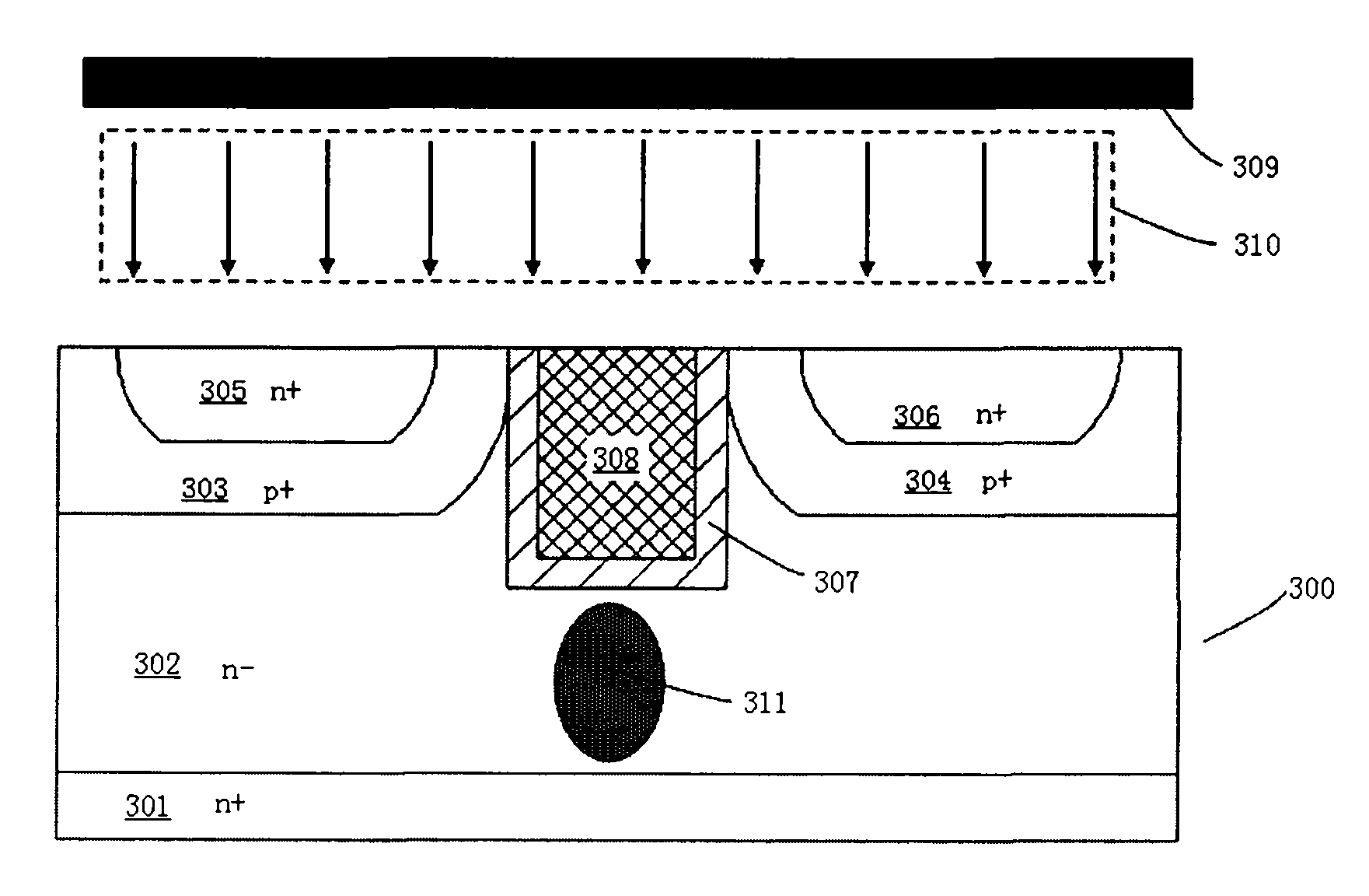
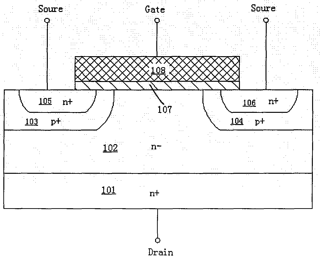
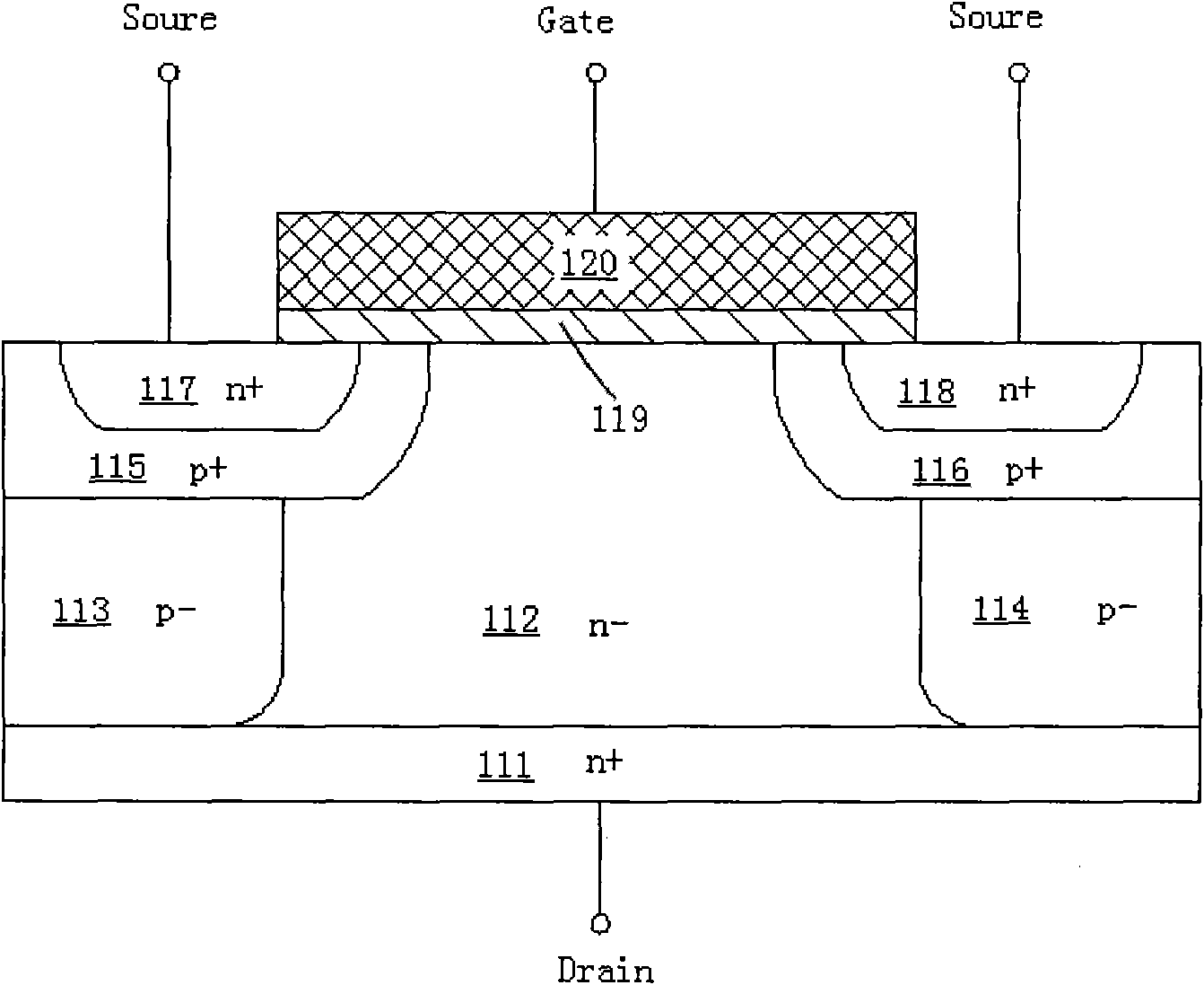
[0020] An exemplary embodiment of the present invention will be described in detail below with reference to the accompanying drawings. In the drawings, the thicknesses of layers and regions are exaggerated for convenience of illustration, and the shown sizes do not represent actual sizes. Although these figures do not completely reflect the actual size of the device, they still fully reflect the mutual positions between the regions and the constituent structures, especially the upper-lower and adjacent relationships between the constituent structures.

[0021] FIG. 2 is a schematic diagram of an operation of conducting conductance modulation of an n-type trench gate power MOS transistor by means of photoelectron injection. As shown in FIG. 2, a light emitting diode (LED lamp) 309 is placed above the substrate surface of the power MOS transistor 300, so that the LED lamp 309 can inject photoelectrons into the MOS transistor 300, and the dotted line box 310 is a schematic diagra...


PUM


Abstract

The invention belongs to the technical filed of semiconductor devices, and in particular discloses a power device and a method for performing conductivity modulation by using photoelectron injection. The power device comprises at least one photoelectron injection light source and a power MOS transistor. By adopting a photoelectron injection method, current carriers are injected into a drift region below the gate of the power MOS transistor and the conductivity modulation is performed, so that the characteristic on-resistance of the power MOS transistor is reduced; and simultaneously the doping concentration of the drift region can be reduced and a blocking-voltage can be improved, so that the performance of the power MOS transistor is greatly improved and the application of the power MOS transistor is expanded to high-voltage fields.

Description

technical field [0001] The invention belongs to the technical field of semiconductor devices, specifically relates to a semiconductor power device, in particular to a power device using photoelectron injection for conductance modulation, and the invention also relates to a method for using photoelectron injection to conduct conductance modulation for a power device. Background technique [0002] In the past 20 years, power devices and their packaging technology have developed rapidly, especially power MOS transistors, which have replaced traditional bipolar transistors in many application fields with their superior characteristics (high input impedance, short turn-off time, etc.). In power circuits, power MOS transistors are mainly used as switching devices. The on-state power consumption of the power MOS transistor is relatively high. To reduce the on-state power consumption, the on-state resistance Rds(on) must be reduced. Conventional power MOS transistors usually adopt ...

Claims


Application Information

Patent Timeline
Patent Type & Authority Applications(China)
IPC IPC(8): H01L29/78H01L29/06
CPCH01L31/1136H01L29/78H01L31/167H01L29/06
Inventor 王鹏飞孙清清丁士进张卫
Owner FUDAN UNIV
Why Eureka
Try Eureka