Method for adjusting angle of oxide field plate in LDMOS transistor

A technology of oxides and transistors, applied in semiconductor devices, semiconductor/solid-state device manufacturing, electrical components, etc., can solve problems such as impact and unsatisfactory effects, improve electrical performance, reduce characteristic on-resistance, and increase breakdown voltage Effect

Pending Publication Date: 2020-10-16
SHANGHAI HUAHONG GRACE SEMICON MFG CORP
View PDF0 Cites 0 Cited by
  • Summary
  • Abstract
  • Description
  • Claims
  • Application Information

AI Technical Summary

Problems solved by technology

At this time, if the angle between the oxide field plate 11 and the semiconductor substrate 10 is too large, after forming a polysilicon structure (such as a polysilicon gate) on the side of the oxide field plate 11, it is easy to form a polysilicon structure (such as a polysilicon gate) on the oxide field plate 11 side. A polysilicon residue a is generated at the side wall A (such as Figure 1b shown); if the angle between the oxide field plate 11 and the semiconductor substrate 10 is too small, the electrical characteristics of the LDMOS transistor such as the breakdown voltage and the characteristic on-resistance (Specific on-Resistance, Rsp) will be affected
[0003] At present, in the LDMOS transistor, in order to obtain the required angle between the oxide field plate 11 and the semiconductor substrate 10, the industry has tried various methods, for example, changing the process parameters of the wet etching (etching time or etching temperature), or utilize UV ​​curing to process the patterned photoresist layer, however, the effect of the above methods is not ideal

Method used


Image

  • Method for adjusting angle of oxide field plate in LDMOS transistor
  • Method for adjusting angle of oxide field plate in LDMOS transistor
  • Method for adjusting angle of oxide field plate in LDMOS transistor

Examples


Embodiment Construction
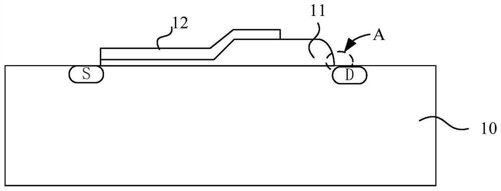
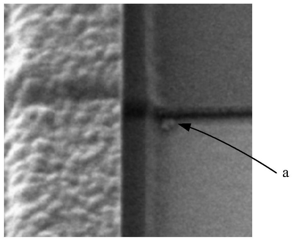
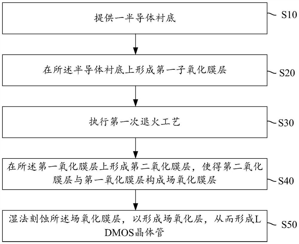
[0038] The core idea of ​​the present invention is to provide a method for adjusting the angle of an oxide field plate in an LDMOS transistor, the method comprising the following steps: providing a semiconductor substrate; forming a first oxide film layer on the semiconductor substrate; performing the first annealing process; forming a second oxide film layer on the first oxide film layer, so that the second oxide film layer and the first oxide film layer form a field oxide film layer; and wet etching the field oxide film layer film layer to form an oxide field plate to form an LDMOS transistor. In the present invention, the first oxide film layer is first formed, and the first annealing process is performed on the first oxide film layer, and then the second oxide film layer is formed, so that the oxide field plate angle during wet etching is controllable That is, the included angle α is between 25° and 75° (preferably, the included angle α is 45°), and this included angle mak...


PUM


Abstract

The invention provides a method for adjusting the angle of an oxide field plate in an LDMOS transistor. The method comprises the following steps: providing a semiconductor substrate; forming a first oxide film layer on the semiconductor substrate; executing a first annealing process; forming a second oxide film layer, so that the second oxide film layer and the first oxide film layer form a fieldoxide film layer; and performing wet etching on the field oxide film layer to form an oxide field plate so as to form the LDMOS transistor. First, the first oxide film layer is formed, the first annealing process is performed on the first oxide film layer; and then the second oxide film layer is formed, so that the angle of the oxide field plate is controllable during wet etching, the included angle enables the problem of polycrystalline silicon residue not to occur during subsequent formation of the field plate on the oxide field plate, the breakdown voltage is improved, the characteristic on-resistance is reduced, and thus the electrical performance of the semiconductor device is improved.

Description

technical field [0001] The invention relates to the field of semiconductor integrated circuit manufacturing, in particular to a method for adjusting the angle of an oxide field plate in an LDMOS transistor. Background technique [0002] The BCD process is a process for fabricating a bipolar junction transistor (Bipolar Junction Transistor, BJT), a complementary metal oxide semiconductor (CMOS), and a diffused metal oxide semiconductor (DMOS) on the same chip. In the process of preparing LDMOS transistors (Laterally Diffused Metal Oxide Semiconductor) transistors using BCD technology, field plates are usually used to reduce the electric field and increase the voltage, such as Figure 1a As shown, the field plate is extended from the polycrystalline gate 12 to straddle the oxide field plate 11 (Field Oxide, FOX, referred to as field oxygen). Generally, a field oxide film layer is formed on the semiconductor substrate 10 by a deposition process first, and then the field oxide f...

Claims


Application Information

Patent Timeline
Patent Type & Authority Applications(China)
IPC IPC(8): H01L21/336H01L29/78H01L29/40
CPCH01L29/402H01L29/66681H01L29/7816
Inventor 吴亚贞
Owner SHANGHAI HUAHONG GRACE SEMICON MFG CORP
Why Eureka
Try Eureka