Method and device for realizing photoelectrochemical micro-etch processing of masked electrode

A photoelectrochemical and processing method technology is applied in the field of photoelectrochemical micro-etching processing methods and devices for mask electrodes, and can solve the problem that the substrate cannot be directly illuminated, the processing fineness is restricted, and the fabrication accuracy of the microprobe electrode affects the substrate. Processing and other problems, to achieve the effect of favorable exclusion, high degree of fineness, and high processing efficiency

Inactive Publication Date: 2010-09-01
JIANGSU UNIV
View PDF5 Cites 36 Cited by
  • Summary
  • Abstract
  • Description
  • Claims
  • Application Information

AI Technical Summary

Problems solved by technology

The manufacturing precision of the microprobe electrode in this method will definitely affect the processing of the substrate, and the achieved processing fineness is restricted by the probe electrode; It can irradiate the gap of the array electrode that does not need to be processed, but cannot directly irradiate the processed part of the substrate facing the electrode

Method used


Image

  • Method and device for realizing photoelectrochemical micro-etch processing of masked electrode
  • Method and device for realizing photoelectrochemical micro-etch processing of masked electrode
  • Method and device for realizing photoelectrochemical micro-etch processing of masked electrode

Examples


Embodiment 1

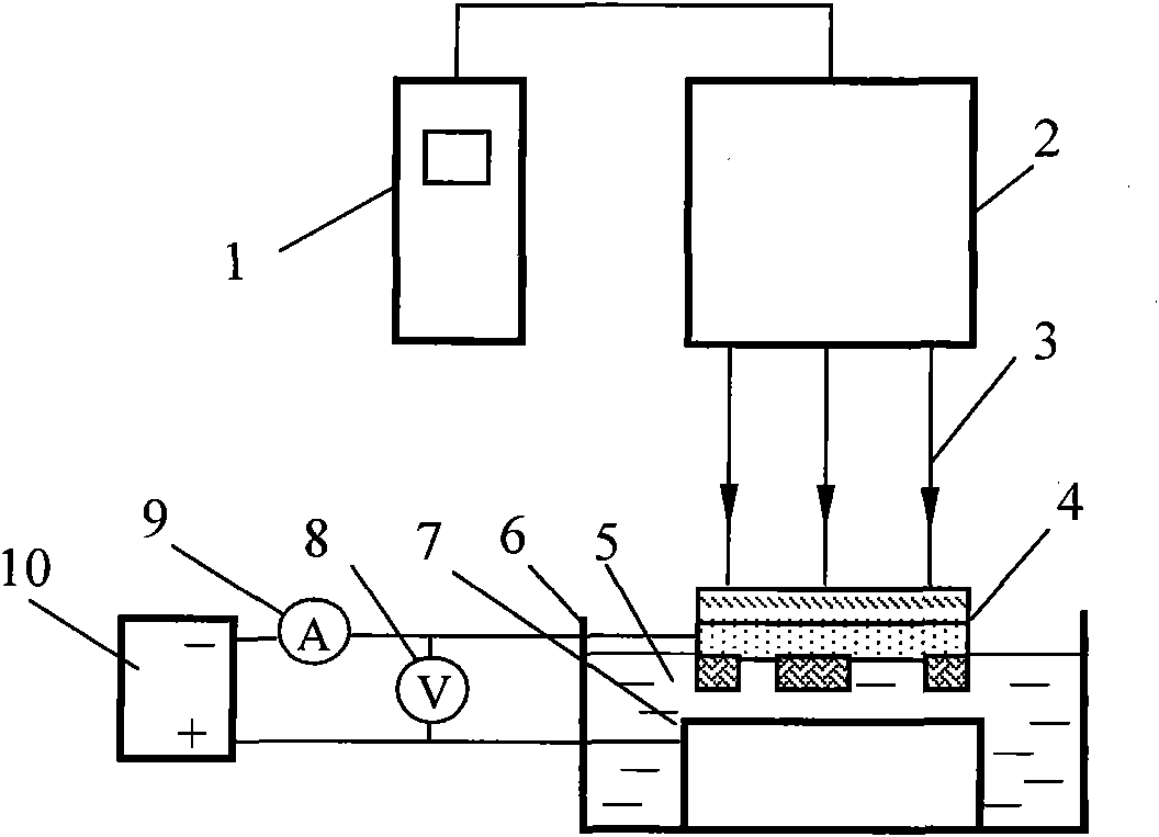
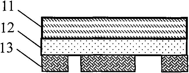
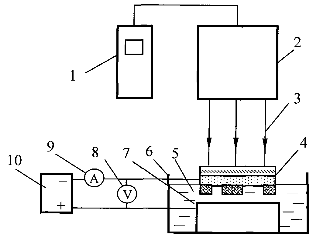
[0026] Embodiment 1: This embodiment is a photoelectrochemical micro-etching processing method of a mask electrode. The first step is to make a mask electrode with a micro-pattern structure. Choose glass with high laser transmittance as the substrate, or coat the upper surface of the glass with an optical antireflection film to make the laser transmittance greater than 95%. The transmittance of the conductive light-transmitting indium tin oxide layer to the laser is greater than 90%, and the resistivity is 1~5×10 -4 Ω / cm. The photoresist layer is mainly composed of photosensitive resin, sensitizer and solvent. The transmittance of the laser beam for processing is less than 15%, and the required fine structure is processed by the photolithography process to serve as a beam mask and The role of electric field masks.

[0027] The laser generates a laser beam 3 with a pulse time of 10 nanoseconds, the laser wavelength is 532 nanometers, the spot mode can be fundamental mode or mult...


PUM

PropertyMeasurementUnit
wavelengthaaaaaaaaaa
electrical resistivityaaaaaaaaaa

Abstract

The invention provides a method and a device for realizing the photoelectrochemical micro-etch processing of a masked electrode, and relates to the micro processing field in the manufacturing technology. A masked electrode used by the invention comprises a glass substrate, an indium tin oxide (ITO) layer and a photoresist mask layer, wherein the conductive light-permeable ITO layer is used as a tool electrode for electrochemical processing and can be permeated by a laser beam, and the photoresist mask layer can limit the action zones of the laser beam and the electrochemical electrode to achieve the double effects of a beam mask and an electric field mask. When the laser beam permeates the masked electrode, a mask pattern is imaged on the surface of a workpiece, the force effect of a shock wave generated by the irradiation of the laser between the workpiece and the electrolyte enables the passivation layer to be removed by the generation of stress corrosion. Meanwhile, the workpiece material at the laser-irradiated part is removed by etching under the action of the photoelectrochemical reaction. The invention can effectively enhance the processing efficiency, the micro processing degree and the processing precision of the complex pattern, and is applicable to the micro processing of the conductive metal material.

Description

Technical field [0001] The invention relates to the field of micro-processing in manufacturing technology, in particular to a photoelectrochemical micro-etching processing method and device of a mask electrode, which is suitable for processing the micro-structure of conductive metal materials. Background technique [0002] With the continuous emergence of high-tech products, the requirements for the function, structural complexity, and reliability of micro devices are getting higher and higher, making the feature sizes from micrometers to millimeters, the use of high-performance materials, and certain shape accuracy and The demand for precision small parts with surface quality requirements is increasingly urgent. After years of hard work and exploration, the processing and manufacturing technology of micro-devices has been greatly developed and has been extended to various modern processing methods. Among them, the laser has the characteristics of high energy, high spatial resol...

Claims


Application Information

Patent Timeline
Patent Type & Authority Applications(China)
IPC IPC(8): B23H5/00
Inventor 张朝阳张永康鲁金忠叶云霞王耀民陈飞
Owner JIANGSU UNIV
Why Eureka
Try Eureka