SiGe heterojunction bipolar transistor and preparation method thereof

A heterojunction bipolar and transistor technology, applied in semiconductor/solid-state device manufacturing, semiconductor devices, electrical components, etc., can solve problems such as incompatibility, and achieve the effect of improving electrical isolation and reducing punch-through

Inactive Publication Date: 2010-09-01
SHANGHAI HUAHONG GRACE SEMICON MFG CORP
View PDF1 Cites 8 Cited by
  • Summary
  • Abstract
  • Description
  • Claims
  • Application Information

AI Technical Summary

Problems solved by technology

Therefore, the use of traditional deep groove technology will not meet the needs of modern technology

Method used


Image

  • SiGe heterojunction bipolar transistor and preparation method thereof
  • SiGe heterojunction bipolar transistor and preparation method thereof
  • SiGe heterojunction bipolar transistor and preparation method thereof

Examples


Embodiment Construction

[0012] In order to illustrate the technical content, structural features, achieved goals and effects of the present invention in detail, the following will be described in detail in conjunction with the embodiments and accompanying drawings.

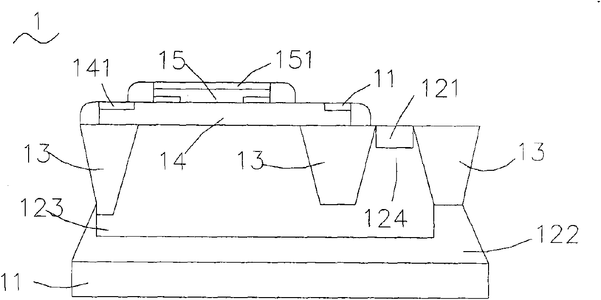
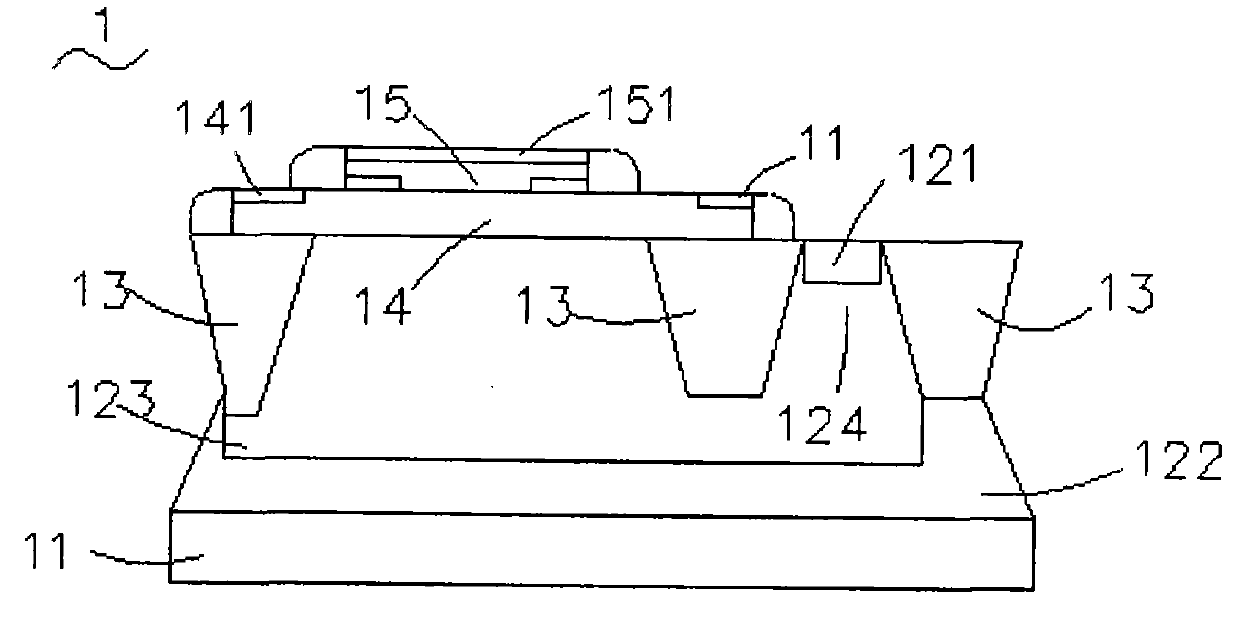
[0013] see figure 2 , figure 2 It is a cross-sectional view of the structure of the first SiGe heterojunction bipolar transistor 1 . The first SiGe heterojunction bipolar transistor 1 includes: a first substrate 11, a first collector region 12 grown on the first substrate 11, and a first shallow collector region 12 formed in the first collector region 12. Trench isolation 13, a first SiGe layer 14 epitaxially grown on the first collector region 12, a first base electrode 141 formed on the first SiGe layer 14, a first emitter region formed on the first SiGe layer 14 15. The first emitter electrode 151 formed on the first emitter region 15 and the first collector electrode 121 formed on the first collector region 12 . Wherein, the fir...


PUM


Abstract

The invention relates to a SiGe heterojunction bipolar transistor which comprises a substrate, a collector region, a shallow groove isolation formed in the collector region, a SiGe layer epitaxially grown on the collector region, a base electrode formed on the SiGe layer, an emitting region formed on the SiGe layer, an emitting electrode formed on the emitting region and a collector electrode formed on the collector region, wherein the collector region further comprises an anti-punchthrough layer formed on the substrate by adopting an ion implantation mode and an n-type buried layer formed on the anti-punchthrough layer, and the anti-punchthrough layer is implanted by a p-type bag region. Through forming the anti-punchthrough layer between the substrate and the collector region, the invention reduces the punchthrough between transistors, enhances the electrical isolation and improves the threshold frequency and the maximum oscillation frequency of the SiGe heterojunction bipolar transistor, and meanwhile, the manufacture cost of the SiGe bipolar transistor is also reduced.

Description

technical field [0001] The invention relates to a semiconductor transistor and a preparation method thereof, in particular to a SiGe heterojunction bipolar transistor and a preparation method thereof. Background technique [0002] Heterojunction bipolar transistor is one of the research focuses of SiGe devices at present. Optimizing the performance of SiGe heterojunction bipolar transistors depends on taking full advantage of the advantages of "doping engineering" and "energy band engineering" in device design and manufacturing. In a SiGe heterojunction transistor, the bandgap of the base material is smaller than that of the emitter, so the doped area does not need to be heavily doped, but the base area can be heavily doped, so that the base area has low resistance, low noise, and high injection efficiency, which can reduce the Tunneling, punch-through and capacitance of the emitter junction. The base area can also be made very thin, which can shorten the transit time of t...

Claims


Application Information

Patent Timeline
Patent Type & Authority Applications(China)
IPC IPC(8): H01L29/737H01L29/08H01L21/331H01L21/762
Inventor 孙涛
Owner SHANGHAI HUAHONG GRACE SEMICON MFG CORP
Why Eureka
Try Eureka