Cover plate structure and manufacturing method thereof, and capacitive sensor

A cover plate and electrical device technology, applied in the field of micro-electromechanical device design and manufacturing, can solve the problems of lack of wide applicability, large parasitic capacitance, high manufacturing cost, etc., achieve no need for high temperature, reduce parasitic capacitance, and good airtightness Effect

Active Publication Date: 2019-04-16
INST OF SEMICONDUCTORS - CHINESE ACAD OF SCI +1
View PDF8 Cites 3 Cited by
  • Summary
  • Abstract
  • Description
  • Claims
  • Application Information

AI Technical Summary

Problems solved by technology

[0005] In the above solution, the entire silicon wafer is used as the substrate or cover plate, and is packaged by direct bonding. The advantage is that the process is relatively simple. The disadvantage is that it uses a high-temperature process and does not have wide applicability. In addition to the detection capacitance formed by the corresponding area of ​​the bottom, the parasitic capacitance formed in other areas is very large; the technology of silicon pillars buried in the middle of the glass is called GIS (GlassinSilicon) technology. First, deep silicon etching is required to form silicon pillars, and then the glass Heating and reflux filling between the silicon columns, and then double-sided grinding and polishing to prepare the GIS cover plate, which has good sealing performance, but the preparation cost is high

Method used


Image

  • Cover plate structure and manufacturing method thereof, and capacitive sensor
  • Cover plate structure and manufacturing method thereof, and capacitive sensor
  • Cover plate structure and manufacturing method thereof, and capacitive sensor

Examples


no. 1 example

[0055] In a first embodiment of the present disclosure, a cover structure in which an insulating material forms a sealed cover is provided.

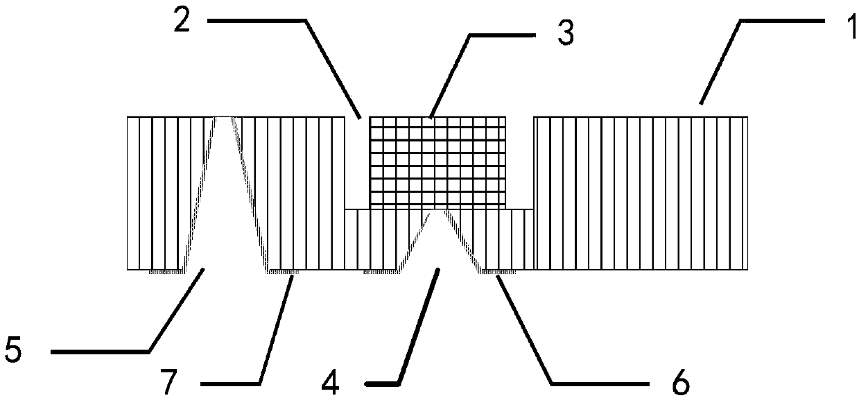
[0056] refer to figure 1 As shown, the cover plate structure shown in this embodiment includes: a sealing cover plate 1 formed of an insulating material, on which a groove 2 is provided, and the groove forms an accommodating space; an electrode plate 3 is located in the groove 2 In the formed accommodating space, there is a gap between the sealing cover plate 1 on the left and right sides of the groove 2; the first vertical through hole 4 is arranged under the electrode plate 3, and passes through the sealing cover plate 1 below the groove 2 The second vertical through hole 5 is arranged on the non-groove position of the sealing cover plate 1 and runs through the sealing cover plate 1; and the first electrode lead 6 and the second electrode lead 7 are respectively along the first vertical through hole 4 and The second vertical through h...

no. 2 example

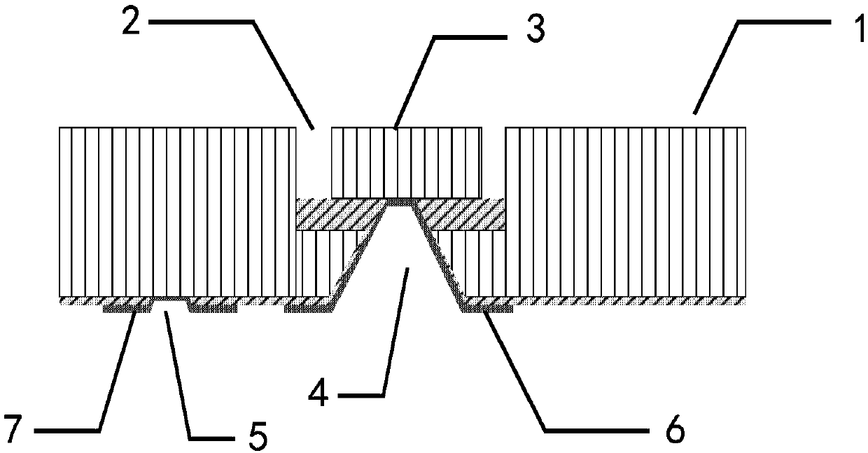
[0068] In a second embodiment of the present disclosure, there is provided a cap structure in which a semiconductor material covered with an insulating material forms a hermetic cap. Compared with the first embodiment, the structure is the same, the difference is that in the cover structure of this embodiment, the material of the sealing cover 1 is a semiconductor material covered with an insulating material, such as silicon covered with silicon oxide.

[0069] refer to figure 2 As shown, the cover plate structure shown in this embodiment includes: a sealing cover plate 1, which is provided with a groove 2, and the groove forms an accommodation space; an electrode plate 3, located in the accommodation space formed by the groove 2 Inside, there is a gap between the sealing cover plate 1 on the left and right sides of the groove 2; the first vertical through hole 4 is arranged under the electrode plate 3 and runs through the sealing cover plate 1 below the groove 2; the second ...

no. 3 example

[0074] In a third embodiment of the present disclosure, a method for manufacturing the cover structure shown in the first embodiment is provided.

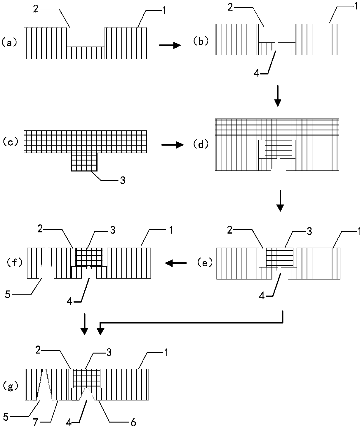
[0075] image 3 It is a schematic flowchart of the manufacturing method of the cover structure according to the third embodiment of the present disclosure.

[0076] refer to image 3 As shown, the manufacturing method of the cover plate structure of the present embodiment includes:

[0077] Step S31: making a groove 2 on the sealing cover plate 1 formed of insulating material, and the groove forms an accommodating space;

[0078] In this embodiment, the sealing cover plate 1 adopts a glass substrate; the upper surface of the glass substrate is patterned and etched to form a groove 2 with a certain depth, such as image 3 Shown in (a).

[0079] Wherein, the etching method is not limited to wet etching, plasma etching, electrochemical etching, etc., and may also include other patterned etching processes.

[0080] Step S32: makin...


PUM

PropertyMeasurementUnit
surface roughnessaaaaaaaaaa

Abstract

The invention discloses a cover plate structure and a manufacturing method thereof, and a capacitive sensor. The cover plate structure is applied to wafer level packaging of micro-electro-mechanical systems, and comprises a sealing cover plate provided with a groove that is formed into an accommodating space; a circuit board positioned in the accommodating space formed by the groove and having gaps with the sealing cover on the left and right sides of the groove; a first vertical through hole arranged under the circuit board and penetrating through the sealing cover plate under the groove; a second vertical through hole arranged in the non-groove position of the sealing cover plate and penetrating through an insulating part in the sealing cover plate; and a first electrode lead and a second electrode lead separately protruded out of the lower surface of the sealing cover plate along the first vertical through hole and the second vertical through hole. The cover plate structure and manufacturing method thereof and the capacitive sensor provided by the invention have the comprehensive performance of being compatible with micro-electro-mechanical system manufacturing technologies, simple in technology and good in gas tightness, having vertical leads, having no use for high temperature, reducing stray capacitance and being wide in application.

Description

technical field [0001] The disclosure belongs to the technical field of design and manufacture of micro-electromechanical devices, and relates to a cover plate structure, a manufacturing method thereof, and a capacitive sensor. Background technique [0002] Micro-electromechanical device (MEMS device) packaging is to seal the movable structure in the chamber to provide support and protection for the movable device, and at the same time, it can connect the electrical signals inside and outside the sealed chamber to drive or detect the action of the micro-electromechanical device. Therefore, the packaging of MEMS devices must simultaneously ensure the airtightness of the package and the electrical interconnection inside and outside the packaging chamber. [0003] According to the movement and detection direction of the structure, MEMS devices can be roughly divided into planar type and vertical type. The movable structure of the planar MEMS device moves in the horizontal direc...

Claims


Application Information

Patent Timeline
Patent Type & Authority Applications(China)
IPC IPC(8): B81B7/00B81B7/02B81C1/00
CPCB81B7/0009B81B7/007B81B7/02B81C1/00015B81C1/00269
Inventor 张萌司朝伟韩国威宁瑾杨富华刘雯颜伟
Owner INST OF SEMICONDUCTORS - CHINESE ACAD OF SCI
Why Eureka
Try Eureka