Circuit and method for resisting SEU of SRAM FPGA device

A circuit and device technology, which is applied in the field of two-dimensional CRC check circuit, enables dynamic reconfigurable hardware to have anti-SEU function in the field of circuit structure, can solve the waste of time and power consumption, cannot check data per frame, and takes a long time to check, etc. problems, to reduce the time and power consumption of reconstruction, to extend the mean time between failures, and to achieve the effect of easy implementation

Active Publication Date: 2010-09-08
FUDAN UNIV
View PDF3 Cites 42 Cited by
  • Summary
  • Abstract
  • Description
  • Claims
  • Application Information

AI Technical Summary

Problems solved by technology

This method can only check one frame of data at a time, and cannot check each frame of data at the same time, and the checking time is longer
Moreover, the programming points where the SEU effect occurs account for a very small proportion of the number of programming points in one frame, and the bit stream of one frame is downloaded each time, resulting in a waste of time and power consumption

Method used


Image

  • Circuit and method for resisting SEU of SRAM FPGA device
  • Circuit and method for resisting SEU of SRAM FPGA device
  • Circuit and method for resisting SEU of SRAM FPGA device

Examples


Embodiment Construction

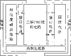
[0029] The anti-SEU circuit proposed by the present invention is valuable in the application of preventing the single event upset effect from causing damage to the hardware based on the SRAM structure, and should cooperate with the overall process to play a role.

[0030] Utilize the anti-SEU circuit that the present invention proposes to implement the concrete steps of anti-SEU error function as Figure 7 As shown, the specific description is as follows:

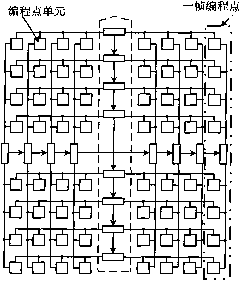
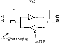
[0031] (1) Fine-grained readback. The programming point information is output to the read-back register through the read-back amplifier, and the output of the frame address decoder and the intra-frame address decoder is controlled by the instruction stored in the FAR register, and the use of the tri-state Buffer of the programming point that needs to be read back The enabling terminal of the tri-state Buffer corresponding to the programming point that does not need to be read back is set to a low level.

[0032] (2) Two-d...


PUM


Abstract

The invention belongs to the technical field of field programmable gate array (FPGA), and particularly relates to a circuit and a method having the function of resisting the single event upset (SEU) effect for an SRAM FPGA device. The SEU-resisting circuit comprises a read-back circuit, a fine-grained refresh circuit and a two-dimensional CRC calibration circuit. A bus state machine controls the read-back circuit to read information stored in a programming point in a read-back register in the read-back circuit, and then, the two-dimensional CRC calibration circuit calibrates the information and writes the address of the programming point generating the SEU effect in an SEU register; and an internal processor generates a fine-grained refreshing bit stream via the fine-grained refresh circuit based on the output of the SEU register, and the refreshing bit stream is written in an internal programming point of the FPGA chip via a self-configuration interface. The programming point generating the SEU error in the FPGA is refreshed again, thereby realizing the SEU-resistant function. Meanwhile, the invention also reduces the time and power consumption for reconstructing the FPGA after the SEU generation.

Description

technical field [0001] The invention belongs to the technical field of field programmable gate arrays, and in particular relates to a circuit structure and a method for enabling dynamic reconfigurable hardware to have anti-SEU functions. In particular, it relates to a two-dimensional CRC check circuit in a SRAM FPGA device, a fine-grained readback and refresh circuit structure and a new anti-SEU method. Background technique [0002] The programmable feature of field programmable gate array (field programmable gate array, FPGA) makes FPGA have great advantages compared with ASIC in terms of time to market, circuit debugging and repeated design. However, the structure of FPGA based on SRAM makes it prone to SEU-single-event upset (SEU-single-event upset) effect and cause circuit logic errors [1]. Based on the FPGA with SRAM structure, the configuration bitstream determines the internal wiring and functions of the designed circuit [2]. Each bit in the bitstream information cor...

Claims


Application Information

Patent Timeline
Patent Type & Authority Applications(China)
IPC IPC(8): G06F11/10
Inventor 谢婧来金梅
Owner FUDAN UNIV
Why Eureka
Try Eureka