System and method of monitoring and diagnosing system condition and performance

a technology of system condition and performance, applied in the field of systems and methods of monitoring and diagnosing functional and/or performance aspects of operations, can solve the problems of not providing sufficient information, unable to preventative measures to be taken, performance failure and/or degradation detected, etc., to save time during fault determination analysis and improve the time to repair

Inactive Publication Date: 2007-01-04
ASML NETHERLANDS BV
View PDF7 Cites 12 Cited by
  • Summary
  • Abstract
  • Description
  • Claims
  • Application Information

AI Technical Summary

Benefits of technology

[0016] Various aspects of the invention overcome at least some of these and other drawbacks of existing systems. According to one embodiment of the invention, the mean time to repair (MTTR) may be improved by providing system performance information. For example, system performance degradation may be correlated with regions of the lithocell that have experienced changes, as measured using performance indicators. By associating system performance degradation to targeted regions of the lithocell, time may be saved during fault determination analysis.

Problems solved by technology

In known systems, performance failure and / or degradation are detected by measuring product wafers or monitor wafers after completion of processing steps.
However, identifying problems after detecting performance failure and / or degradation does not allow preventative measures to be taken.
Waiting until completion of processing steps to measure product wafers or monitor wafers for performance failure and / or degradation may not provide sufficient information to determine a source of the failure.
Diagnosing failure is complex at least because cause and effect are not one-to-one related.
This analysis is not efficient and may consume a considerable amount of time, especially when all potential causes are explored in a pre-selected order, without the benefit of targeted problem-solving techniques.
Known methods of waiting until completion of processing steps to measure product wafers or monitor wafers for performance failure and / or degradation are also deficient because they do not enable monitoring of devices for performance failures and / or degradations by detecting drifts and / or failure modes at an early stage.
Rather, known methods detect performance failures and / or degradations after they have occurred.
However, the lithocell may deliver defective product wafers or monitor wafers at the end of processing steps even if one or more individual sensor readings are determined to be within an acceptable working range.
The defective wafers may result from an actual performance of sensor / actuator systems, wherein the performance is acceptable in isolation but unacceptable when coupled to other sensor / actuator systems.
Other drawbacks exist with these and other conventional systems.

Method used


Image

  • System and method of monitoring and diagnosing system condition and performance
  • System and method of monitoring and diagnosing system condition and performance
  • System and method of monitoring and diagnosing system condition and performance

Examples


Embodiment Construction

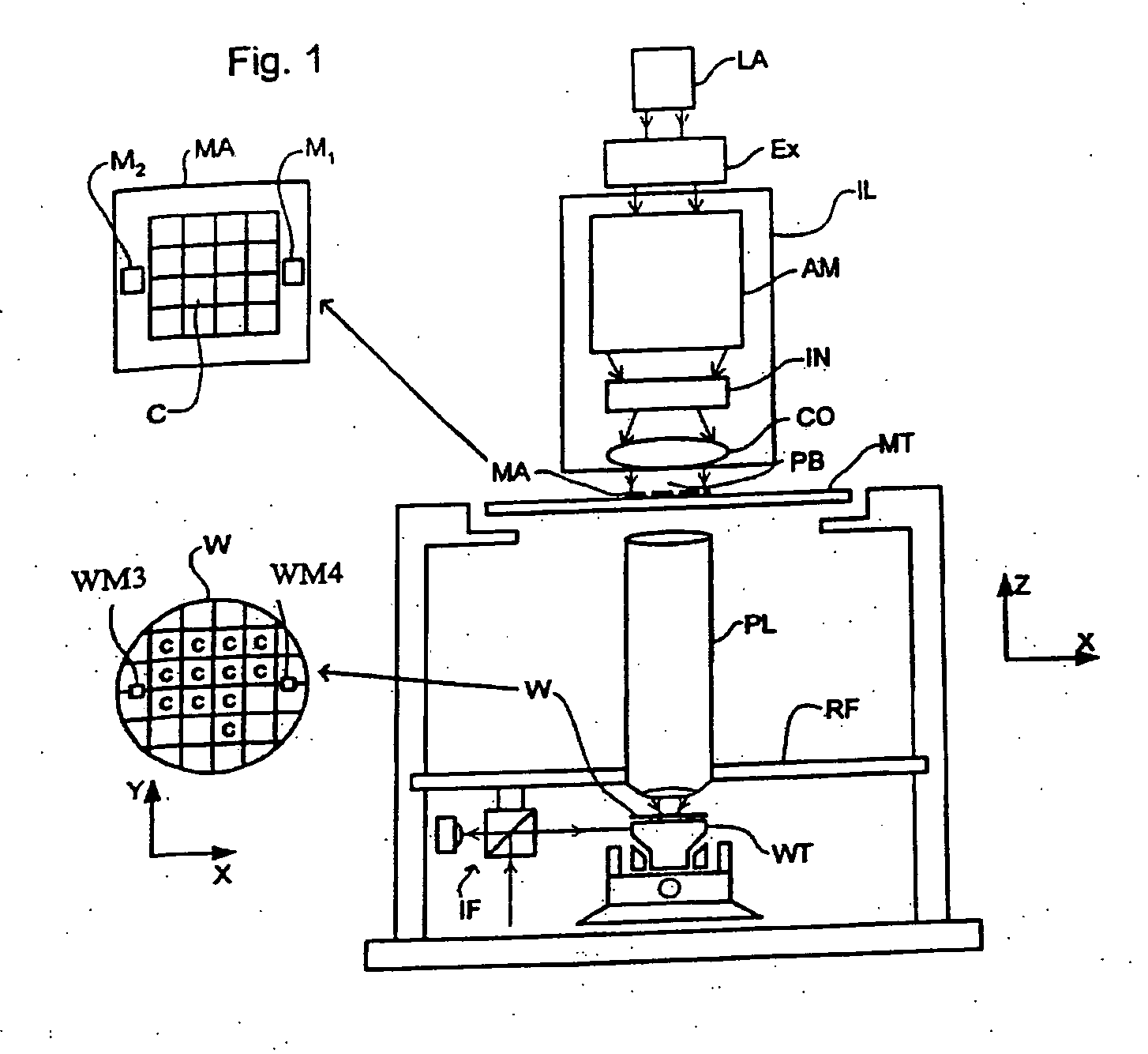
[0032]FIG. 1 schematically depicts a lithographic apparatus according to a particular embodiment of the invention. The apparatus includes an illumination system (illuminator) IL for providing a projection beam PB of radiation (e.g. UV radiation or DUV radiation); a first support structure (e.g. a mask table) MT for supporting patterning structure (e.g. a mask) MA and connected to first positioner PM for accurately positioning the patterning structure with respect to item PL; a substrate table (e.g. a wafer table) WT for holding a substrate (e.g. a resist-coated wafer) W and connected to second positioner PW for accurately positioning the substrate with respect to item PL; and a projection system (e.g. a refractive projection lens) PL mounted on a frame F and configured to image a pattern imparted to the projection beam PB by patterning structure MA onto a target portion C (e.g. comprising one or more dies) of the substrate W.

[0033] As here depicted, the apparatus is of a transmissi...


PUM


Abstract

The invention is directed to a system and method of monitoring and/or diagnosing tool performance in real-time for system degradation. The invention issues alerts and provides a structured process for identifying the source of the problem and enabling action to be taken before defects are detected on the final product. The invention provides a hierarchical data structure including elements that are monitored based on key performance indicators and diagnostic data sets.

Description

BACKGROUND [0001] 1. Field of the Invention [0002] This invention relates to systems and methods of monitoring and diagnosing functional and / or performance aspects of operations. [0003] 2. Background Information [0004] A lithographic apparatus is a machine that applies a desired pattern onto a substrate, usually onto a target portion of the substrate. A lithographic apparatus can be used, for example, in the manufacture of integrated circuits (ICs). In that instance, a patterning device, which is alternatively referred to as a mask or a reticle, may be used to generate a circuit pattern to be formed on an individual layer of the IC. This pattern can be transferred onto a target portion (e.g. including part of, one, or several dies) of a substrate (e.g. a silicon wafer or other wafer). The pattern is typically transferred via imaging onto a layer of radiation-sensitive material (resist) provided on the substrate. [0005] In general, a single substrate will contain a network of adjacen...

Claims


Application Information

Patent Timeline
Patent Type & Authority Applications(United States)
IPC IPC(8): G03B27/42
CPCG03F7/70525G03F7/70483
Inventor REUHMAN-HUISKEN, MARIA ELISABETHLEVASIER, LEON MARTINVAN RHEE, TASJASALPIETRO, ROSARIASCHOEMAKER, ERIK JOHANNESJACQMIN, ERICPRINS, MARTINVAN KERVINCK, MARCEL NICOLAAS JACOBUSBOOTSMA, TIMOTHEUS MARC VINCENT
Owner ASML NETHERLANDS BV
Why Eureka
Try Eureka