Array substrate and manufacturing method thereof and liquid crystal panel and manufacturing method thereof

A manufacturing method and technology of array substrates, which are applied in semiconductor/solid-state device manufacturing, optics, instruments, etc.

Active Publication Date: 2012-05-30
BOE TECH GRP CO LTD +1
View PDF4 Cites 0 Cited by
  • Summary
  • Abstract
  • Description
  • Claims
  • Application Information

AI Technical Summary

Problems solved by technology

[0007] The object of the present invention is to provide an array substrate and its manufacturing method, a liquid crystal panel and its manufacturing method, so as to overcome the damage or damage of the gate insulating film and passivation film in the prior art cracking defect

Method used


Image

  • Array substrate and manufacturing method thereof and liquid crystal panel and manufacturing method thereof
  • Array substrate and manufacturing method thereof and liquid crystal panel and manufacturing method thereof
  • Array substrate and manufacturing method thereof and liquid crystal panel and manufacturing method thereof

Examples


no. 1 example

[0057] image 3 It is a flow chart of the first embodiment of the manufacturing method of the array substrate of the present invention. Such as image 3 As shown, the manufacturing method of the array substrate of the present invention includes:

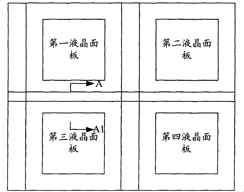
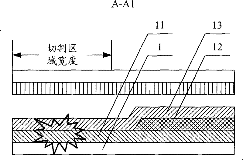
[0058] Step 101, providing a substrate, the substrate includes a plurality of liquid crystal panel regions and a plurality of cutting regions, the cutting regions are located between adjacent liquid crystal panel regions, so as to isolate each of the liquid crystal panel regions;

[0059] Step 102, forming gate lines and gate electrodes on the substrate;

[0060] Step 103, depositing a gate insulating film on the substrate on which the gate lines and gate electrodes are formed, and forming an active layer, data lines, source electrodes, drain electrodes and channels on the gate electrodes;

[0061] Step 104, depositing a passivation film on the substrate on which the data line, source electrode, drain electrode and channel are for...

no. 3 example

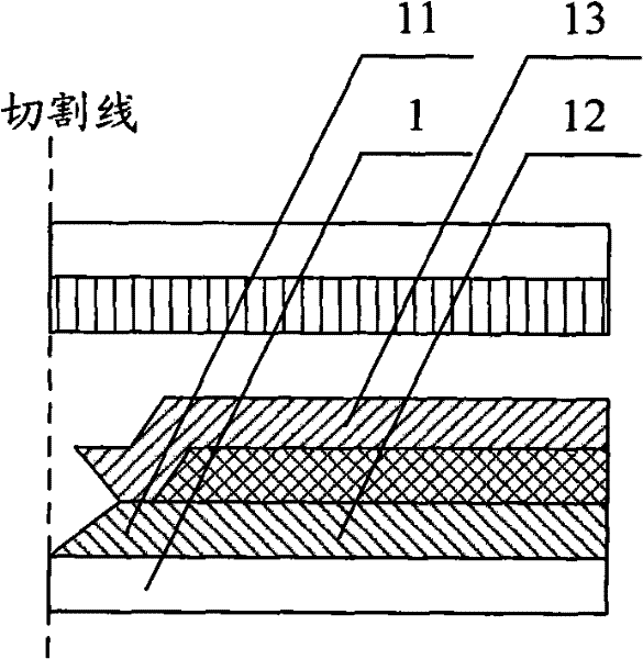
[0074] Figure 5a It is a flow chart of the third embodiment of the manufacturing method of the array substrate of the present invention. Figure 5b It is a schematic diagram of the substrate provided in the third embodiment of the manufacturing method of the array substrate of the present invention. Figure 5c It is a schematic diagram of forming gate lines and gate electrodes in the third embodiment of the manufacturing method of the array substrate of the present invention. Figure 5d It is a schematic diagram of forming an active layer, a data line, a source electrode and a drain electrode in the third embodiment of the manufacturing method of the array substrate of the present invention. Figure 5e It is a schematic diagram of forming a passivation layer via hole and a pixel electrode in the third embodiment of the manufacturing method of the array substrate of the present invention. Figure 5f It is a schematic diagram of removing the gate insulating film and the passi...


PUM


Abstract

The invention relates to an array substrate and a manufacturing method thereof and a liquid crystal panel and a manufacturing method thereof. The array substrate comprises a display area and a non-display area, wherein the non-display area comprises a cutting area and other areas, the other areas are provided with a double-layer structure which is formed by a grid insulation film and a passivation film, and the cutting area exposes the substrate. During the cutting process, the defects such as the breakage or fracture of the grid insulation film and the passivation film can be effectively overcome.

Description

technical field [0001] The invention belongs to the field of liquid crystal display devices, and in particular relates to an array substrate and a manufacturing method thereof, a liquid crystal panel and a manufacturing method capable of preventing damage or cracking of a gate insulating film and a passivation film during a cutting process. Background technique [0002] A liquid crystal display device (Liquid Crystal Display, referred to as LCD) is a main flat panel display device (Flat Panel Display, referred to as FPD). [0003] Liquid crystal display devices are classified into vertical electric field type liquid crystal display devices and horizontal electric field type liquid crystal display devices according to the direction of an electric field for driving liquid crystals. Vertical electric field type liquid crystal display devices include: twisted nematic (TwistNematic, referred to as TN) type liquid crystal display devices; horizontal electric field type liquid crys...

Claims


Application Information

Patent Timeline
Patent Type & Authority Patents(China)
IPC IPC(8): H01L21/84H01L21/311H01L21/78H01L27/12G02F1/1362
Inventor 朴相镇
Owner BOE TECH GRP CO LTD
Why Eureka
Try Eureka