Light emitting device

A technology for light-emitting devices and light-emitting modules, applied in electrical components, electrical solid-state devices, circuits, etc., can solve the problems of false welding, cumbersome and labor-intensive, hindering heat dissipation, etc.

Active Publication Date: 2010-09-08
BRIGHT LED ELECTRONICS CORP
View PDF0 Cites 2 Cited by
  • Summary
  • Abstract
  • Description
  • Claims
  • Application Information

AI Technical Summary

Problems solved by technology

[0003] Since the light emitting diodes 10 of this light emitting module 1 must be soldered on the circuit board 12 by arrangement and reflow soldering, subsequent assembly and application can be performed. Not only does there exist the problem of false soldering, but it is also cumbersome and laborious to manufacture. The high temperature generated in the reflow soldering process is also easy to damage the light emitting diode 10 and is not conducive to batch production; and moreover, when the light emitting diode 10 is soldered on the circuit board 12, the contact between the light emitting diode and the circuit board is poor or there is a gap that hinders heat dissipation. , causing the temperature of the light-emitting diode to be high, shortening the normal service life
[0004] It can be seen that the above-mentioned existing light-emitting devices obviously still have inconvenience and defects in structure and use, and need to be further improved urgently.
In order to solve the above-mentioned problems, the relevant manufacturers have tried their best to find a solution, but no suitable design has been developed for a long time, and the general products do not have an appropriate structure to solve the above-mentioned problems. This is obviously related. The problem that the industry is eager to solve

Method used


Image

  • Light emitting device
  • Light emitting device
  • Light emitting device

Examples


Embodiment Construction

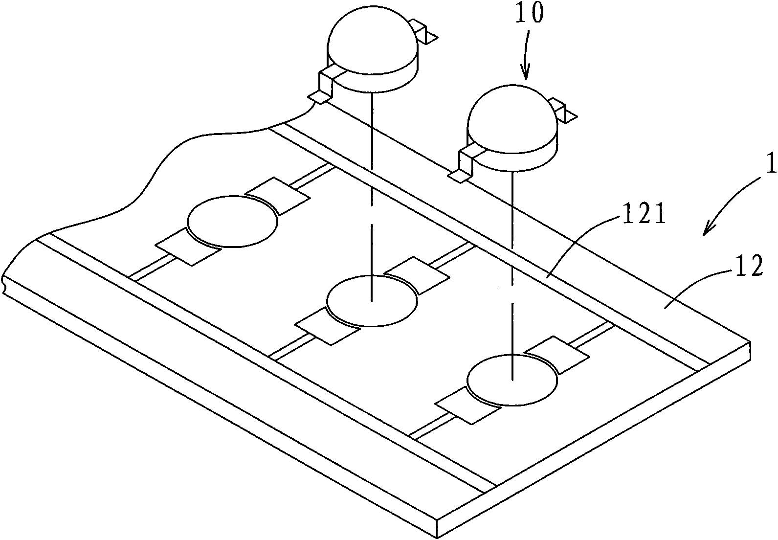
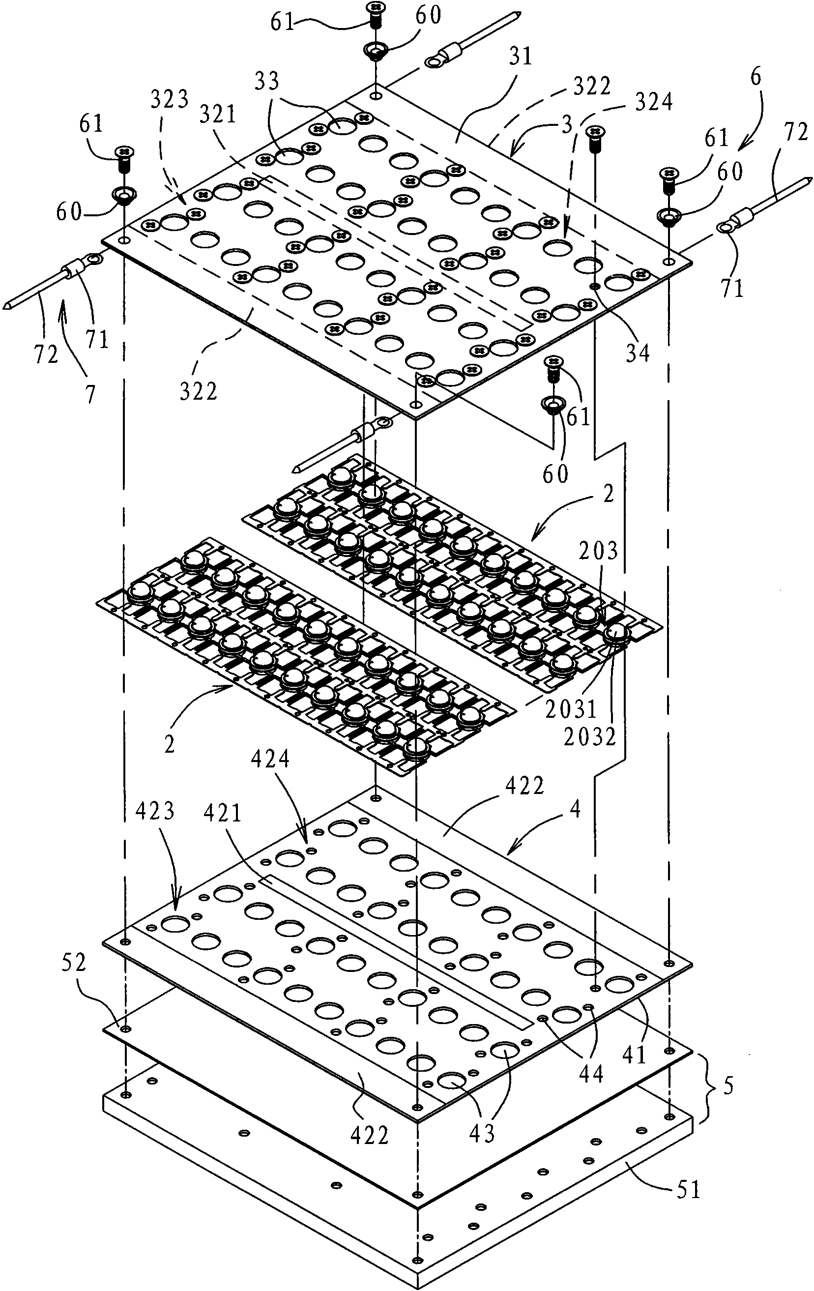
[0043] In order to further explain the technical means and effects adopted by the present invention to achieve the intended purpose of the invention, the specific implementation, structure, features and effects of the light-emitting device proposed according to the present invention will be described in detail below in conjunction with the accompanying drawings and preferred embodiments. The description is as follows.

[0044] The aforementioned and other technical contents, features and effects of the present invention will be clearly presented in the following detailed description of preferred embodiments with reference to the drawings. Through the description of the specific implementation mode, when the technical means and functions adopted by the present invention to achieve the predetermined purpose can be obtained a deeper and more specific understanding, but the accompanying drawings are only for reference and description, and are not used to explain the present inventi...


PUM


Abstract

The invention relates to a light emitting device comprising a light emitting module, a first conducting plate and a heat radiating plate set. The light emitting module comprises a conducting circuit consisting of one metal sheet and a plurality of light emitting diodes, the plurality of light emitting diodes are arranged on the conducting circuit and are connected in series and parallel by the conducting circuit, and the light emitting module can be locked between the first conducting plate and the heat radiating plate set and can be externally connected with an outside power source by contacting with a conducting area on the first conducting plate. Because the construction of the light emitting module and the locking combination between the light emitting module and the first conducting plate do not need a process of welding with a circuit board or reflow soldering, the manufacturing process is simpler, and the impaction and the breakage of the light emitting diode, caused by high temperature generated during the welding or reflow soldering process, can be avoided, so that it is beneficial to the batch production; in addition, the bottom of the light emitting diode is in forced, direct and efficient contact with a heat conducting layer on the heat radiating plate set by strong mechanical pressure, the heat conducting layer thins, the head transfer effect is better, and it is beneficial to the radiation of the light emitting diode, thus the normal service life of the light emitting diode can be maintained.

Description

technical field [0001] The invention relates to a light-emitting device, in particular to a lead frame with a light-emitting diode packaged therein, which can simplify the manufacturing process, avoid high temperature damage to the light-emitting diode during reflow soldering, facilitate batch production, and ensure that the light-emitting diode has a good performance. The light-emitting device that can maintain the normal service life of the light-emitting diode by the heat dissipation. Background technique [0002] see figure 1 As shown, it is a perspective view of a conventional light-emitting module. A conventional light-emitting module (a module is a module, referred to as a module herein) 1 includes a circuit board 12 (or a metal substrate) on which a conductive line 121 is laid on the surface. or ceramic substrate) and a plurality of chips are used to arrange the light emitting diodes 10 soldered on the circuit board 12 . In the conventionally known light-emitting m...

Claims


Application Information

Patent Timeline
Patent Type & Authority Applications(China)
IPC IPC(8): H01L25/075H01L23/367H01L21/50
CPCH01L24/97H01L2924/0002H01L2924/12041
Inventor 曾庆霖张铭利林政杰
Owner BRIGHT LED ELECTRONICS CORP
Why Eureka
Try Eureka