High voltage semiconductor device

A semiconductor and device technology, applied in the field of medium/high voltage semiconductor devices, can solve the problems of limited and high cost of semiconductor devices

Inactive Publication Date: 2010-09-08
NXP BV
View PDF0 Cites 14 Cited by
  • Summary
  • Abstract
  • Description
  • Claims
  • Application Information

AI Technical Summary

Problems solved by technology

[0009]Therefore, due to the relatively poor on-resistance versus breakdown voltage trade-off, high cost due to additional processing steps and / or masking, device One or more problems related to the risk of failure, existing semiconductor devices are limited in application

Method used


Image

  • High voltage semiconductor device
  • High voltage semiconductor device
  • High voltage semiconductor device

Examples


Embodiment Construction

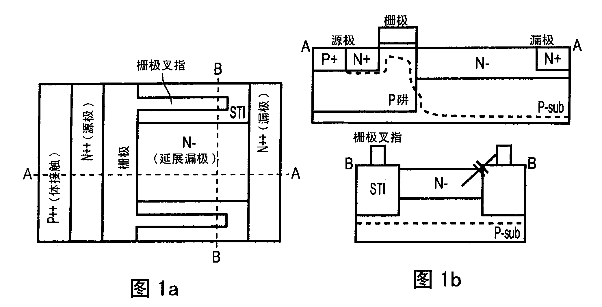
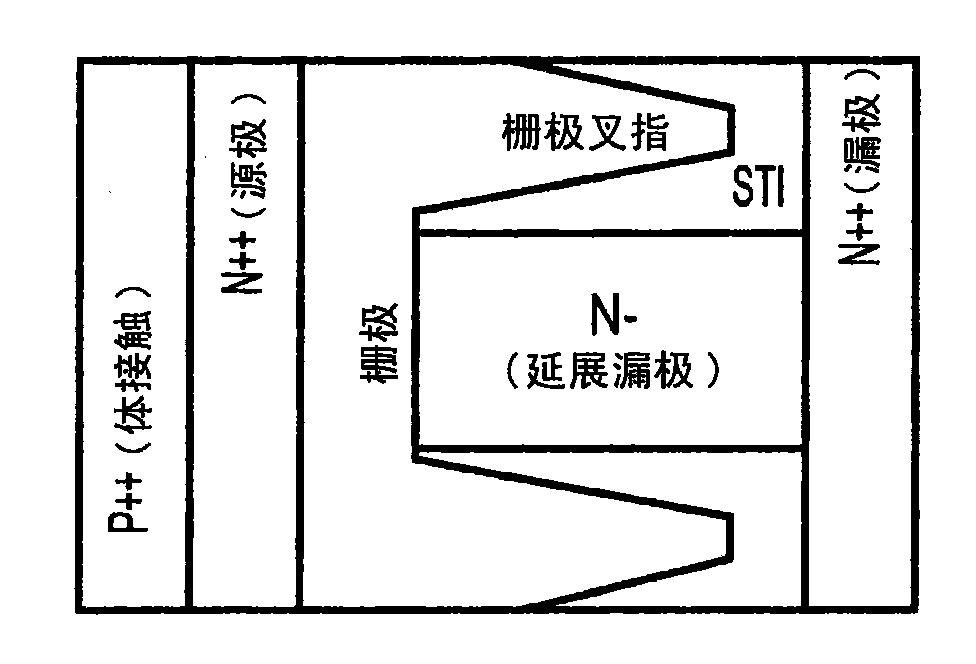
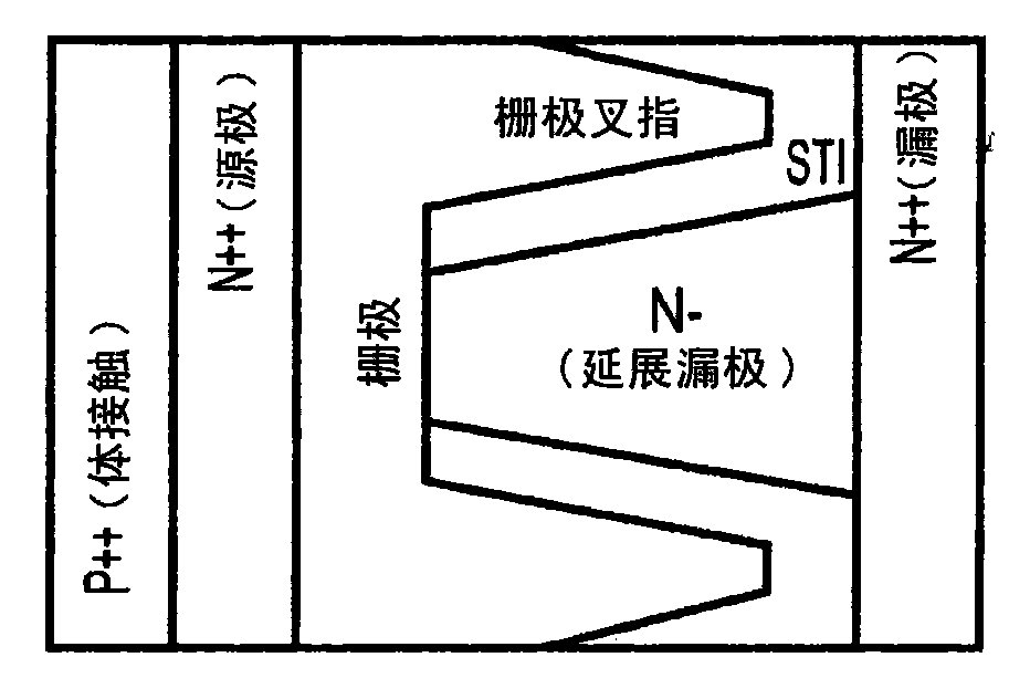
[0047] In a first aspect, the present invention relates to a semiconductor device for high-voltage applications, comprising at least one dielectric in a substrate region, preferably an STI region, and one or more semiconductor regions located between the at least one dielectric region One or more conductive extensions located on the side surface of the at least one dielectric region and extending on the at least one dielectric region, wherein the one or more extensions pass through the dielectric region at the edge of the extension and the dielectric The part between the edges capacitively interacts with the one or more semiconductor regions.

[0048] In the IC process, these conductive extensions can be most conveniently realized as gate (doped polysilicon) extensions. In the following description, they can also be called gate fingers, polysilicon fingers, gate field plates or Polysilicon field plate.

[0049] Semiconductor devices are particularly suitable for most CMOS processe...


PUM


Abstract

This invention describes implementation of medium / high voltage semiconductor devices with a better voltage-blocking capability versus specific on-resistance trade off. This approach can be implemented in baseline and submicron CMOS without any additional process steps. CMOS semiconductor devices, such as transistors, are known. Typically these 5 devices have only limited applicability in high voltage (HV) due to for instance breakdown of voltage. Many IC (Integrated Circuit) applications require for instance power management units for DC:DC down-or up-conversion of the supply voltage. Typically NMOS and PMOS semiconductor devices, such as transistors, with capability from10 V up 10 to 25 V are required for such applications.

Description

Technical field [0001] The present invention describes a method for realizing a medium / high voltage semiconductor device with better voltage blocking capability versus characteristic on-resistance trade-off. This method does not require any additional process steps and can be implemented in baseline and sub-micron CMOS. Background technique [0002] CMOS semiconductor devices such as transistors are known. Typically, due to effects such as voltage breakdown, such devices have only limited applications under high voltage (HV). [0003] Most IC (integrated circuit) applications require power management units for DC:DC up-down conversion of power supplies. Typically, for this application, NMOS and PMOS semiconductor devices such as transistors with the ability to rise from 5V to 25V are required. [0004] In addition, applications such as solid-state lighting, power amplifiers, and MEMS sensor or actuator drive circuits require transistors that can handle voltages up to 50v, and even...

Claims


Application Information

Patent Timeline
Patent Type & Authority Applications(China)
IPC IPC(8): H01L21/329H01L21/331H01L21/336H01L29/423H01L29/78H01L29/861H01L29/40H01L29/739
CPCH01L29/66659H01L29/42364H01L29/7824H01L29/7816H01L29/6609H01L29/0653H01L29/66325H01L29/66681H01L29/861H01L29/402H01L29/42356H01L29/4238H01L29/7835
Inventor 简·雄斯基安科·黑林格
Owner NXP BV
Why Eureka
Try Eureka