Semiconductor manufacturing apparatus
A technology for manufacturing devices and semiconductors, which is applied in the field of semiconductor manufacturing devices, can solve problems such as inability to have uniform plasma density, and achieve uniform plasma density
- Summary
- Abstract
- Description
- Claims
- Application Information
AI Technical Summary
Problems solved by technology
Method used
Image

Examples
no. 1 approach
[0034] Embodiments of the present invention will be described with reference to the drawings.
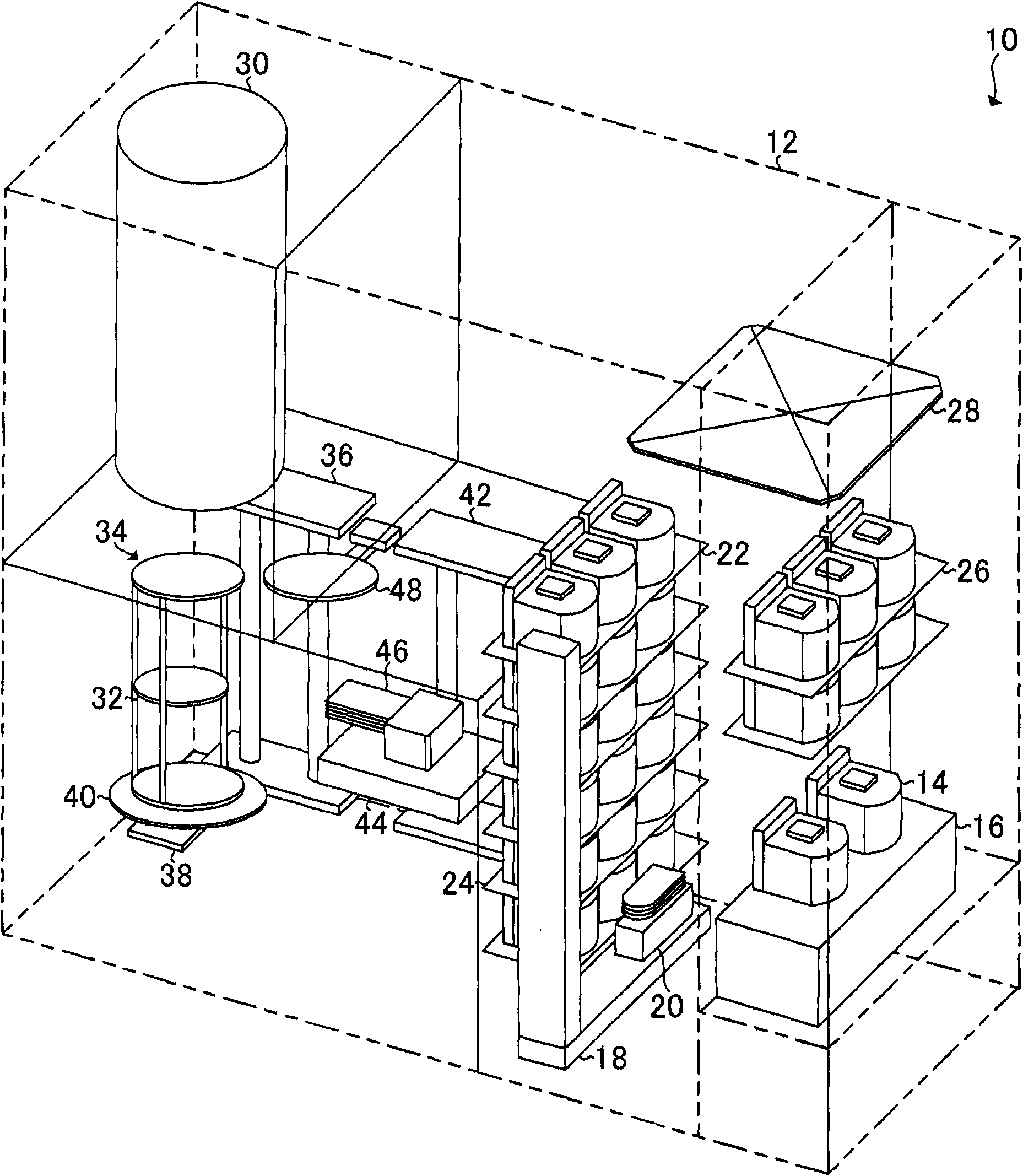
[0035] figure 1 It is a perspective perspective view which shows the semiconductor manufacturing apparatus 10 which is one Embodiment of this invention. This semiconductor manufacturing apparatus 10 is a batch-type vertical semiconductor manufacturing apparatus, and has a housing 12 in which main parts are arranged. On the front surface side of the frame body 12, a cassette stage 16 is provided as a holding member delivery member, and the cassette stage 16 performs the transfer of the cassette 14 as a substrate storage container with an external conveying device (not shown). After delivery, a cassette lifter 18 as a lifting mechanism is provided on the rear side of the cassette mounting table 16 , and a cassette transfer machine 20 as a transport mechanism is attached to the cassette lifter 18 . In addition, a cassette holder 22 serving as a mounting mechanism for the cassettes 14...
no. 2 approach
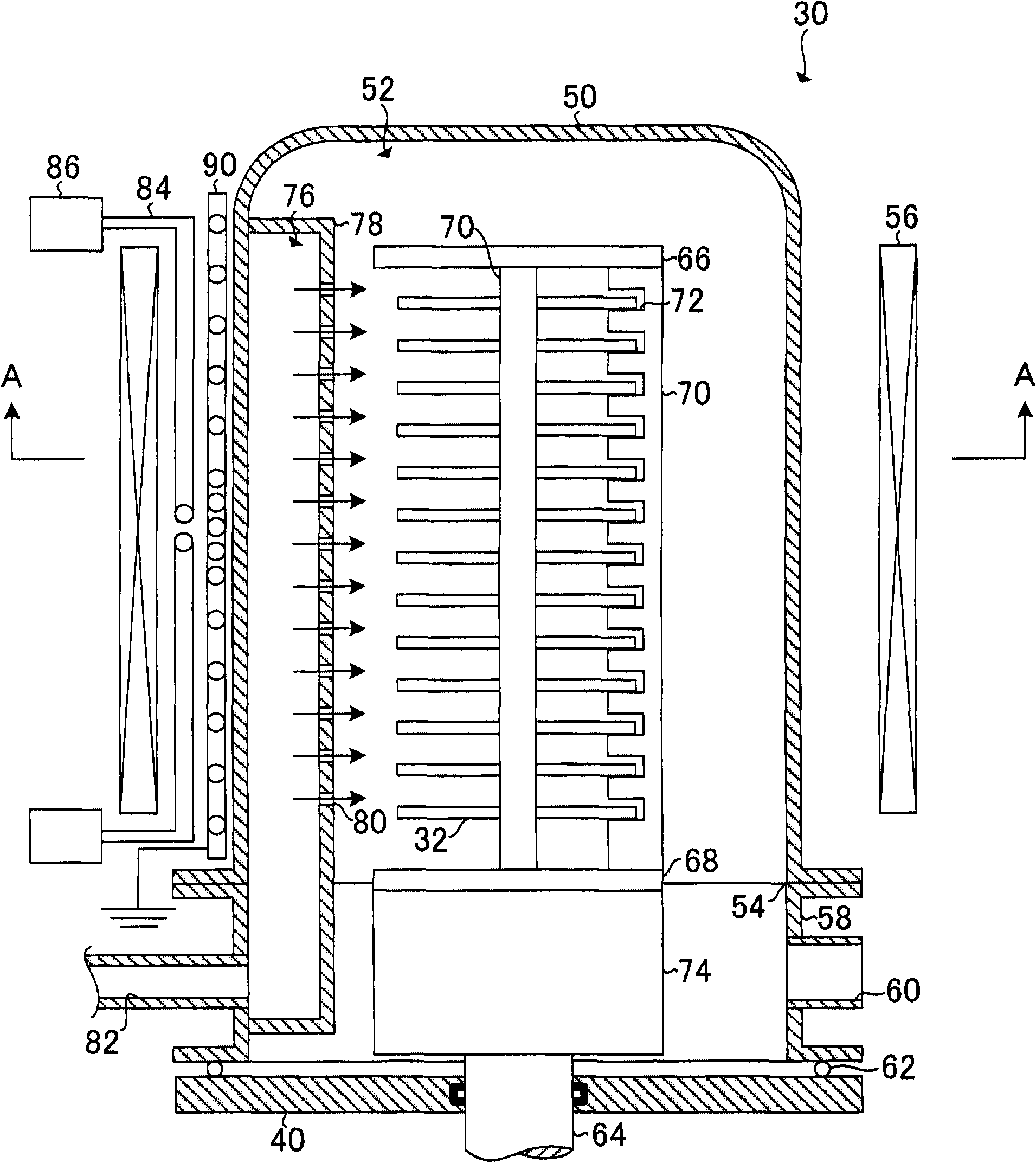
[0061] Figure 5 The surrounding structure of the radio frequency antenna 84 used in another embodiment is shown. Figure 5 (a) briefly shows the front side of the radio frequency antenna 84, Figure 5 (b) shows the surrounding structure of the side surface of the radio frequency antenna 84 . In addition, in Figure 5 The illustration of the shield case 90 is omitted in FIG. In the present embodiment, the high-frequency antenna 84 is bent in a direction away from the plasma chamber 76 at a portion (position P) close to the two high-frequency antennas 84 .
[0062] With the above configuration, the high-frequency antenna 84 is separated from the plasma chamber 76 at the approach portion (position P), so that the force for generating plasma can be adjusted. Accordingly, it is possible to prevent the plasma density generated in the vicinity of the access portion (position P) from increasing, and to make the plasma density generated in the plasma chamber 76 uniform.
no. 3 approach
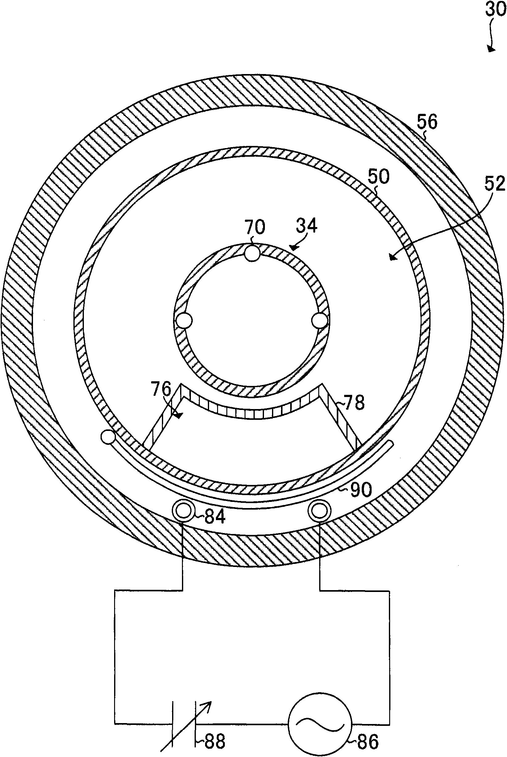
[0064] Image 6 The surrounding structure of the radio frequency antenna 84 used in another embodiment is shown. Image 6 (a) briefly shows the front side of the radio frequency antenna 84, Image 6 (b) shows the surrounding structure of the side surface of the radio frequency antenna 84 . In addition, in Image 6 The illustration of the shield case 90 is omitted in FIG. In the present embodiment, an antenna shield 92 is attached to the high-frequency antenna 84 at a close portion (position P) of the two high-frequency antennas 84 . The antenna shield 92 is formed on the high-frequency antenna 84 via an insulator, for example, and grounds the cylindrical or helical conductor individually. In addition, it is also possible to ground the shield case 90 .
[0065] With the above configuration, the shielding force at the approach portion (position P) is improved, and the force for generating plasma can be adjusted. Accordingly, it is possible to prevent the plasma density gen...
PUM
 Abstract
Description
Claims
Application Information
 - R&D
- Intellectual Property
- Life Sciences
- Materials
- Tech Scout
- Unparalleled Data Quality
- Higher Quality Content
- 60% Fewer Hallucinations
Browse by: Latest US Patents, China's latest patents, Technical Efficacy Thesaurus, Application Domain, Technology Topic, Popular Technical Reports.
© 2025 PatSnap. All rights reserved.Legal|Privacy policy|Modern Slavery Act Transparency Statement|Sitemap|About US| Contact US: help@patsnap.com