High-heat-dispersion spherical array encapsulation method

An array packaging and high heat dissipation technology, which is applied in the manufacture of electrical components, electric solid devices, semiconductor/solid state devices, etc., can solve the problems of poor heat dissipation, semiconductor packaging, poor heat dissipation effect of resin, and inconspicuous heat dissipation effect, and achieve stress absorption The function is beneficial, the package structure is compact, and the effect of meeting the ultra-high heat dissipation requirements

Active Publication Date: 2012-05-02
NANTONG FUJITSU MICROELECTRONICS
View PDF0 Cites 0 Cited by
  • Summary
  • Abstract
  • Description
  • Claims
  • Application Information

AI Technical Summary

Problems solved by technology

[0004] 2. Metal wires are used to realize the packaging structure of electrical interconnection. Most of the chips are bonded to the carrier board through polymer epoxy resin materials. The heat dissipation effect of the resin itself is poor, and the chip mainly conducts heat through the metal particles added in the resin. In order to achieve a better heat dissipation effect, a synthetic resin with a high proportion of metal particles is selected, resulting in a relative decrease in the proportion of the resin, which reduces the bonding force between it and the chip and the carrier board, and then occurs due to weak bonding force. , Reliability issues such as delamination caused by high stress residue caused by high proportion of metal particles
[0005] 3. For semiconductor packages with poor heat dissipation due to the limitation of their own packaging structure, high thermal conductivity plastic packaging materials are also used to improve the heat dissipation effect. However, in addition to the high cost price of high thermal conductivity plastic packaging materials, the control of product packaging technology higher requirements, and the heat dissipation effect is not obvious

Method used


Image

  • High-heat-dispersion spherical array encapsulation method
  • High-heat-dispersion spherical array encapsulation method
  • High-heat-dispersion spherical array encapsulation method

Examples


Embodiment Construction

[0041] Below in conjunction with specific embodiment, further illustrate the present invention. It should be understood that these examples are only used to illustrate the present invention and are not intended to limit the scope of the present invention. In addition, it should be understood that after reading the teachings of the present invention, those skilled in the art can make various changes or modifications to the present invention, and these equivalent forms also fall within the scope defined by the appended claims of the present application.

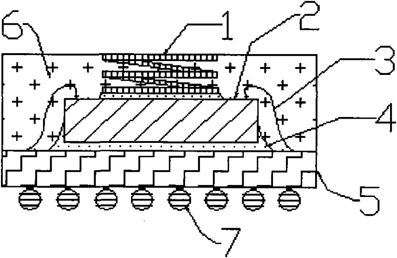
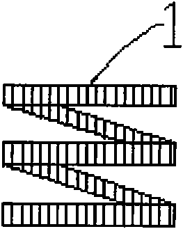
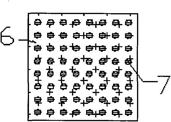
[0042] Embodiments of the present invention relate to a high heat dissipation ball array packaging method, using this method to form a figure 1 The package structure shown includes a chip 2, metal leads 3, bonding material 4, substrate 5, molding compound 6 and solder balls 7, and the package structure also includes a spring radiator 1; the chip 2 is bonded The material 4 is placed on the substrate 5, and is electrically inter...


PUM


Abstract

The invention relates to a high-heat-dispersion reverse solder spherical array encapsulation method which comprises the following steps of: implanting a chip into a substrate by using a binding material; pasting a spring radiator on the chip; electrically connecting the chip and the substrate by a metal lead; plastically encapsulating the spring radiator, the chip, the metal lead, the binding material and the substrate with a plastic encapsulating material to form a plastic encapsulated body; and fixing the periphery of the spring radiator by the plastic encapsulating material, wherein one end of the spring radiator is connected with the chip, and the other end is exposed out of the surface of the encapsulated body so that the heat of the chip is dispersed out of the encapsulated body. The invention solves the problems of heat dispersion in encapsulation without an exposed metal carrier plates and greatly improves the electrothermal performance and the reliability of the product.

Description

technical field [0001] The invention relates to a heat dissipation structure packaging method in the technical field of semiconductor packaging, in particular to a high heat dissipation ball array packaging method. Background technique [0002] The traditional semiconductor flip-chip packaging structure mostly dissipates heat through the substrate, which mainly has the following shortcomings: [0003] 1. With the continuous development of semiconductor technology, there are more and more mid-to-high-end packages that use plastic substrate materials as the chip carrier base. In particular, ball array packages mostly use substrate materials. However, due to the poor thermal conductivity of the plastic substrate itself, heat dissipation not effectively. [0004] 2. Metal wires are used to realize the packaging structure of electrical interconnection. Most of the chips are bonded to the carrier board through polymer epoxy resin materials. The heat dissipation effect of the resi...

Claims


Application Information

Patent Timeline
Patent Type & Authority Patents(China)
IPC IPC(8): H01L21/50H01L23/367
CPCH01L24/97H01L2924/15311H01L2224/48091H01L2224/45124H01L2224/73265H01L2224/48227H01L2224/32225H01L2924/19105H01L2924/30107H01L2224/45147H01L2224/45144H01L2224/97
Inventor 吴晓纯陶玉娟
Owner NANTONG FUJITSU MICROELECTRONICS
Why Eureka
Try Eureka