Manufacturing process for plugging conductive holes of circuit board with resin

A technology of resin plugging and manufacturing process, which is applied in the direction of electrical connection formation of printing components, etc., can solve the problems of difficult air bubbles and difficult to polish clean, and achieve the effect of solving the easy generation of air bubbles, facilitating the polishing process, and improving efficiency

Inactive Publication Date: 2010-10-06
SHENZHEN SUNTAK MULTILAYER PCB
View PDF4 Cites 31 Cited by
  • Summary
  • Abstract
  • Description
  • Claims
  • Application Information

AI Technical Summary

Problems solved by technology

But in the filling process, it is difficult to effectively overcome the problem of air bubbles; and when gri

Method used


Image

  • Manufacturing process for plugging conductive holes of circuit board with resin
  • Manufacturing process for plugging conductive holes of circuit board with resin

Examples


Example Embodiment

[0022] The present invention will be further described in detail below in conjunction with the drawings and specific embodiments.

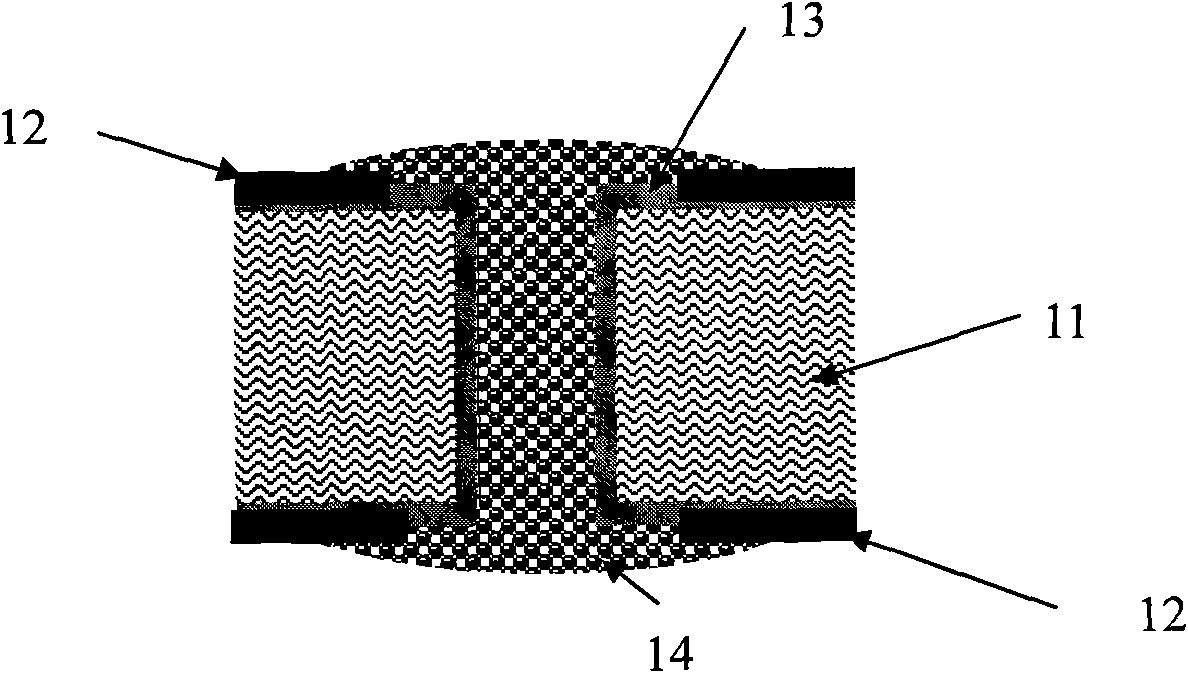
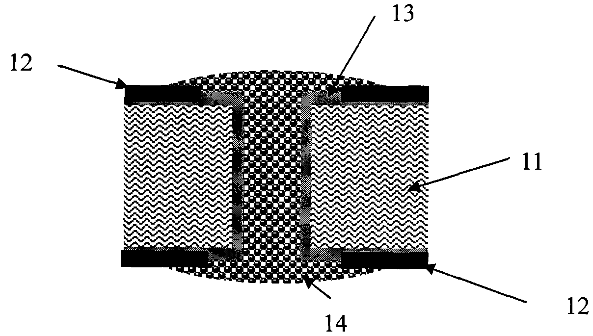
[0023] figure 1 For the circuit board in the resin filling process through the resin plugging process for the conductive holes of the circuit board described in this embodiment, in the figure, 11 is the circuit board substrate, 12 is the dry film, 13 is the window, and 14 is Filled with epoxy resin. The resin plugging is performed through the resin plugging manufacturing process for the conductive holes of the circuit board described in this embodiment, and the specific process is as follows:

[0024] The circuit board substrate with conductive holes is copper-immersed, and the copper-immersed substrate is electroplated; the conductive holes of the electroplated circuit board substrate are windowed, and the window is set with a single side size of 0.10 To 0.20mm tin ring; paste dry film transfer printed graphics on the substrate after opening the win...


PUM


Abstract

The invention discloses a manufacturing process for plugging conductive holes of a circuit board with resin, which comprises the following steps: A) carrying out plated through hole and electroplating treatment on a circuit board substrate which is provided with conductive holes; B) carrying out windowing treatment on conductive holes of the circuit board substrate which is electroplated, and adhering a dry film to transfer the printed picture; C) electroplating the conductive holes of the circuit board which is provided with the dry film; D) filling resin into the conductive holes so as to plug the conductive holes, and baking the circuit board at low temperature after the conductive holes are plugged; E) removing the remained resin through polishing way; F) removing the film of the circuit board after being polished; and G) and baking the circuit board at high temperature after the film is removed. The process not only can solve the problem that the air bubbles are easy to produce by directly filling ink or other anti-corrosion materials, but also greatly reduces the polishing difficulty; and during the hole plugging process of the conductive holes of the circuit board, the circuit board is only required to be polished for one time, so not only the efficiency is improved, but also the cost is reduced.

Description

technical field [0001] The invention belongs to the technical field of circuit board (PCB) manufacturing technology, and in particular relates to the manufacturing technology of the circuit board in which conductive holes need to be filled in double-layer or multi-layer circuit boards. Background technique [0002] With the current development of electronic technology, the manufacturing process of printed circuit boards, which are almost indispensable in electronic products, has also been greatly developed, from single-layer boards to double-layer boards, until now the most commonly used multi-layer boards. When manufacturing double-layer boards, especially multi-layer boards, it is necessary to isolate the metal layer to connect the printed circuits of each layer, so it is necessary to design corresponding conductive holes in the metal base layer. The conductive hole must be filled, otherwise, during the subsequent processing of the circuit board, especially during wave sol...

Claims


Application Information

Patent Timeline
IPC IPC(8): H05K3/40H05K3/42
Inventor 刘东
Owner SHENZHEN SUNTAK MULTILAYER PCB
Why Eureka
Try Eureka