
Process of 0.5mum vertical JFET (Junction Field-effect Transistor)

A process and epitaxial layer technology, applied in electrical components, semiconductor/solid-state device manufacturing, circuits, etc., can solve the problems of low chip integration, large device size, poor device performance, etc., to improve integration and reduce device size. , to ensure the effect of good performance

Inactive Publication Date: 2010-10-13
ADVANCED SEMICON MFG CO LTD
View PDF0 Cites 1 Cited by
  • Summary
  • Abstract
  • Description
  • Claims
  • Application Information

AI Technical Summary

Problems solved by technology

[0002] Traditional vertical JFET devices are manufactured by implanting impurities and advancing them at high temperatures to reach the required vertical depth, but lateral diffusion occupies valuable area while reaching the vertical depth, resulting in large device size and low chip integration. Poor device performance, low breakdown voltage

Method used


Image

  • Process of 0.5mum vertical JFET (Junction Field-effect Transistor)
  • Process of 0.5mum vertical JFET (Junction Field-effect Transistor)

Examples


Embodiment Construction

[0035] The invention discloses a 0.5-micron vertical JFET process. After growing an epitaxial layer on a substrate, grooves are opened in the region where doping is required, and doping implantation is performed in the grooves. The doping implantation is of the opposite type to that of sinking the bottom and the epitaxial layer. s material.

[0036] In one embodiment, the groove is realized by photolithography process, and further includes smoothing the sidewall of the groove.

[0037] In one embodiment, the substrate is an N-type heavily doped substrate, and the epitaxial layer is an N-type lightly doped epitaxial layer. Doping implantation is to implant P-type polysilicon or epitaxial layer.

[0038] In one embodiment, the 0.5 micron vertical JFET process further includes forming the source by photolithography.

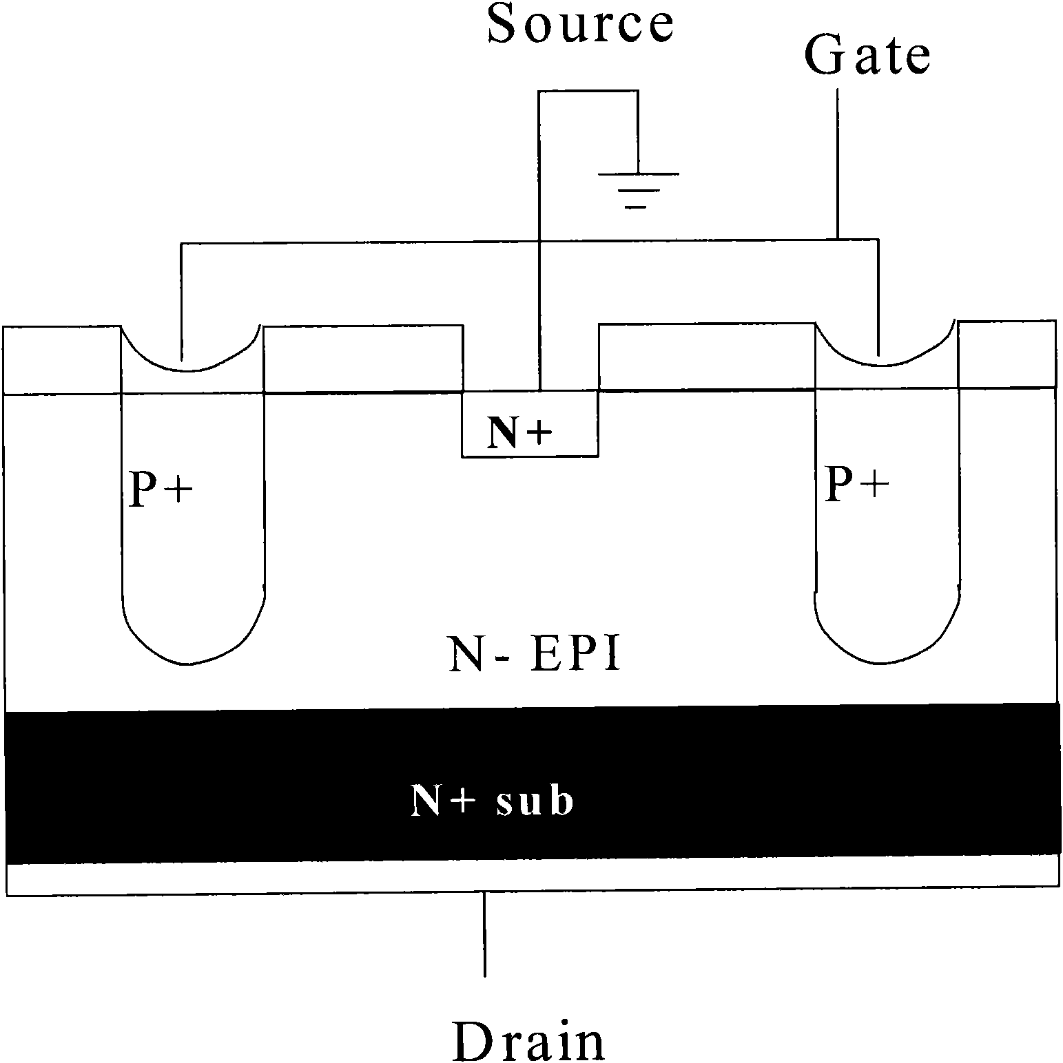
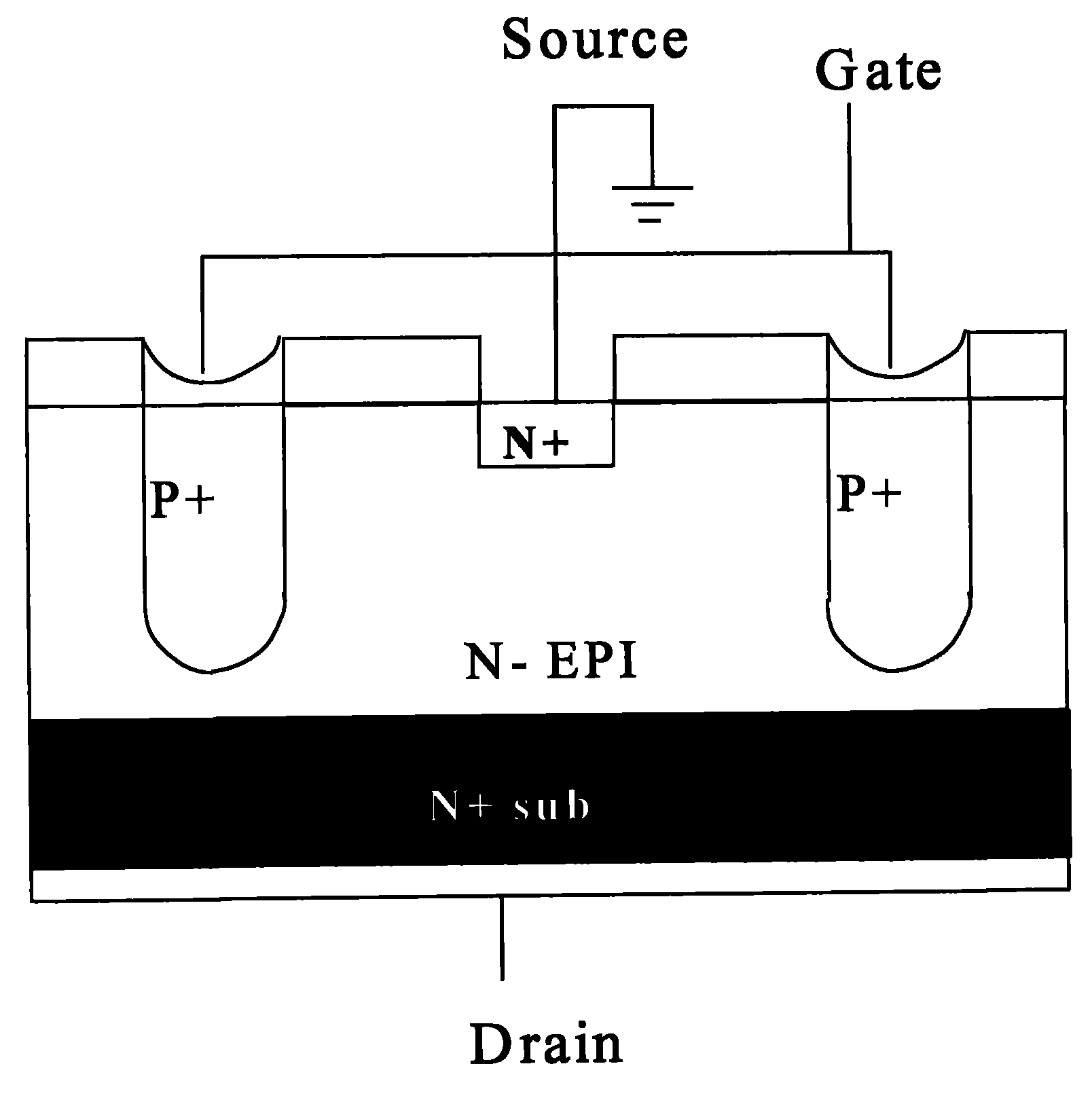
[0039] refer to figure 1 as shown, figure 1 A structural diagram of a JFET device fabricated according to the 0.5 micron vertical JFET process of the present in...


PUM


Abstract

The invention discloses a process of a 0.5 mum vertical JFET (Junction Field-effect Transistor). After an epitaxial layer grows on a substrate, a notch is arranged in an area needing doping, injection doping is carried out in the notch, and the type of material used for the injection doping is opposite to that of the substrate and the epitaxial layer. By adopting the technical scheme of the invention, the transverse diffusion phenomenon is greatly reduced through the notch, the size of a device is reduced, the minimum key size can be reduced to 0.5 mu m, and the integrated level of a chip is improved. In addition, the doping concentration of fillers can be more uniform through the notch, and the favorable performance of the device is ensured.

Description

technical field [0001] The invention relates to a semiconductor manufacturing process, more specifically, to a 0.5 micron vertical JFET process. Background technique [0002] Traditional vertical JFET devices are manufactured by implanting impurities and advancing them at high temperatures to reach the required vertical depth, but lateral diffusion occupies valuable area while reaching the vertical depth, resulting in large device size and low chip integration. The device performance is poor and the breakdown voltage is low. Contents of the invention [0003] The present invention proposes a method of opening and filling polysilicon of the opposite doping type or epitaxy, thereby greatly reducing the lateral diffusion. [0004] According to the present invention, a 0.5 micron vertical JFET process is proposed. After the epitaxial layer is grown on the substrate, grooves are opened in the region where doping is required, and doping implantation is performed in the grooves....

Claims


Application Information

Patent Timeline
IPC IPC(8): H01L21/337H01L21/306H01L21/20H01L21/283
Inventor 刘启星汪大祥孔天午
Owner ADVANCED SEMICON MFG CO LTD
Learn More