Method for manufacturing nano-wire piezoelectric device

A piezoelectric device and manufacturing method technology, applied in the manufacture/assembly of piezoelectric/electrostrictive devices, semiconductor/solid-state device manufacturing, electrical components, etc., can solve the problem of low output power, nanogenerator wear, nanowire and Electrode wear and other problems, to achieve the effect of improving stability and output power, wide application range and simple production process

Inactive Publication Date: 2010-10-13
SUZHOU INST OF NANO TECH & NANO BIONICS CHINESE ACEDEMY OF SCI
View PDF3 Cites 15 Cited by
  • Summary
  • Abstract
  • Description
  • Claims
  • Application Information

AI Technical Summary

Problems solved by technology

Although the vertical generator has achieved great success and derived models based on different substrates, its further development still faces some difficulties that need to be resolved urgently
One challenge comes from the precise control of the distance between the driving electrodes and the ZnO nanowires, a small amount of error can cause the generator not to work properly
In addition, when the vertical generator is working, the free en

Method used


Image

  • Method for manufacturing nano-wire piezoelectric device
  • Method for manufacturing nano-wire piezoelectric device
  • Method for manufacturing nano-wire piezoelectric device

Examples


Embodiment Construction

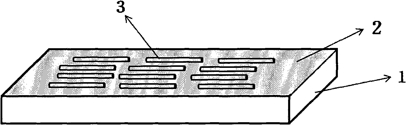
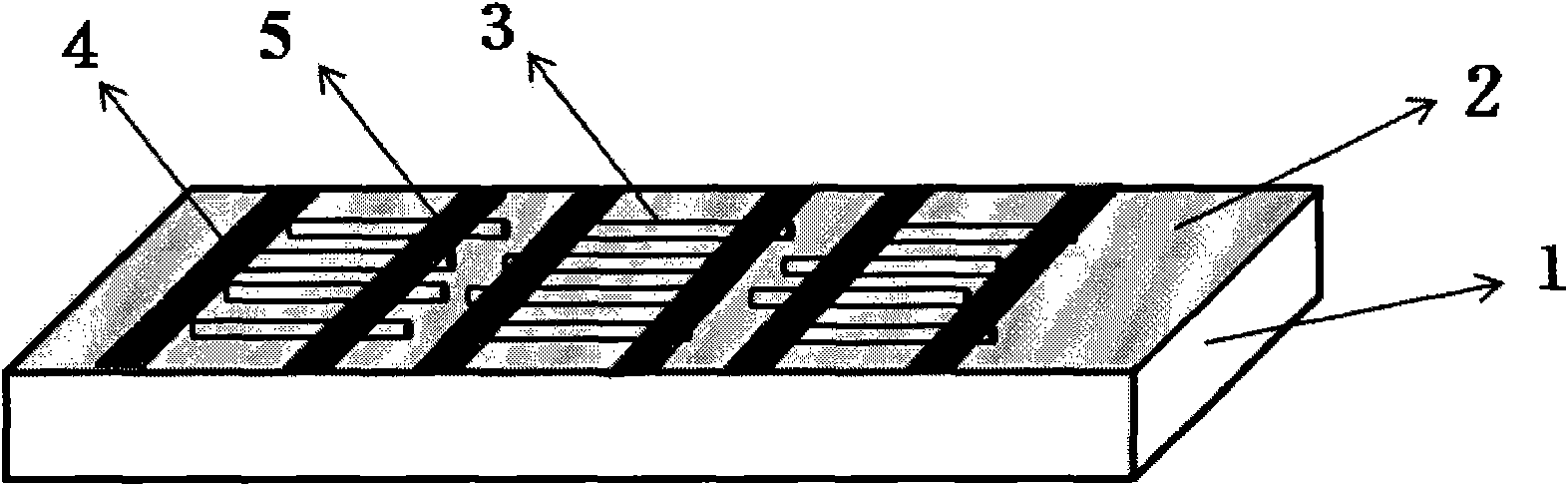
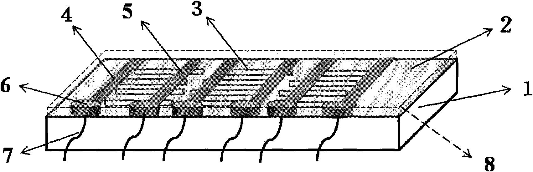
[0026] The invention provides a fabrication and integration method of a large-area parallel arrangement nanowire piezoelectric device. First, a large-area parallel array of nanowires was prepared on the surface of the polyimide film by direct dry transfer method; then, metal source-drain electrodes were prepared on the surface of the above-mentioned nanowire array by using the standard micro-nano lithography process. Next, the metal contacts of the source and drain electrodes are grouted, and the surface of the piezoelectric device is encapsulated with polydimethylsiloxane (PDMS) after the leads are drawn from the contacts, so as to be connected and tested with the outside. Since a large number of nanowires can work simultaneously to convert mechanical energy into electrical energy; therefore, the present invention has better stability and higher output power than a single nanowire piezoelectric device. At the same time, this method is compatible with the traditional semicondu...


PUM


Abstract

The invention discloses a method for manufacturing a nano-wire piezoelectric device, which comprises the following steps of: arranging prefabricated nano-wires on a polyimide film to form parallel nano-wire arrays by using direct dry transfer; preparing a source electrode and a drain electrode of the piezoelectric device on the nano-wire arrays by adopting a micro or nano photo-etching method; and finally, adding a connecting point and a lead for connection on one side of the source electrode and one side of the drain electrode, and packing the surface of the piezoelectric device by adopting polydimethylsiloxane. The manufacturing method has the advantages of simple manufacturing process, wide application range, cost saving and the like, and greatly improves the yield of the piezoelectric device; the nano-wire piezoelectric device manufactured by implementing the method can realize simultaneous work of a large amount of nano-wires to generate electrical energy; and the stability and the output power of the piezoelectric device are improved by combining a packing process.

Description

technical field [0001] The invention relates to a method for manufacturing a nano device, in particular to a method for manufacturing a piezoelectric device in which nano wires are arranged in parallel in a large area, and belongs to the related fields of nano technology and semiconductor electronic technology. Background technique [0002] As an important emerging scientific and technological field in the 21st century, nanotechnology is experiencing rapid development in theory and practice. A large number of new nanomaterials and devices have been developed continuously, and have shown unprecedented application prospects in various fields of biomedicine, national defense and people's daily life. However, with the development of nanotechnology to this day, a large amount of research has focused on the development of high-sensitivity, high-performance nano-devices, and there is almost no research on power systems at the nanoscale. However, the demand for such a power supply ...

Claims


Application Information

Patent Timeline
IPC IPC(8): H01L21/782H01L41/22H01L41/23
Inventor 文燎勇邵铮铮金朝边历峰
Owner SUZHOU INST OF NANO TECH & NANO BIONICS CHINESE ACEDEMY OF SCI
Why Eureka
Try Eureka