Membrane stress testing structure and method as well as manufacturing method

A technology for film stress and test structure, which is applied in the direction of microstructure technology, microstructure devices, chemical instruments and methods, etc., can solve the problems of inability to reflect stress characteristics, calculate film stress, and Poisson's ratio is not completely determined, and achieve the test structure The effect of small size, simple measuring tool and simple process

Active Publication Date: 2010-10-27
北方广微科技有限公司
View PDF0 Cites 14 Cited by
  • Summary
  • Abstract
  • Description
  • Claims
  • Application Information

AI Technical Summary

Problems solved by technology

[0010] However, many of the materials used in MEMS are non-standard materials, and their Poisson's ratio is often unknown or incompletely determined, and will not be integrated in the software of the stress tester.
Even though the strain gauge can still measure the radius of curvature of the film optically, it cannot calculate the stress of the film using the Stoney formula
[0011] This method has another disadvantage: the measured stress is for the film on the entire wafer and cannot reflect the stress characteristics of a local area

Method used


Image

  • Membrane stress testing structure and method as well as manufacturing method
  • Membrane stress testing structure and method as well as manufacturing method
  • Membrane stress testing structure and method as well as manufacturing method

Examples


Embodiment Construction

[0043] Specific embodiments of the present invention will be described in detail below. It should be noted that the embodiments described here are for illustration only, and are not intended to limit the present invention.

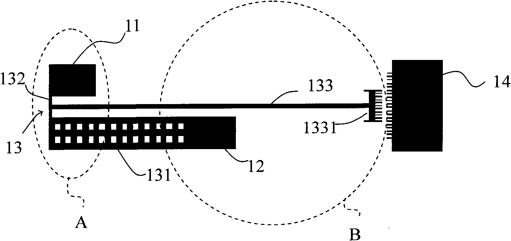
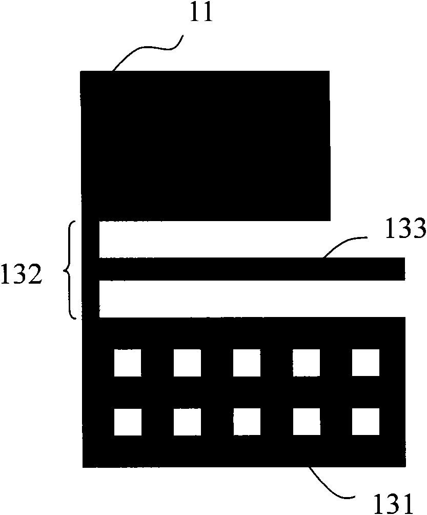
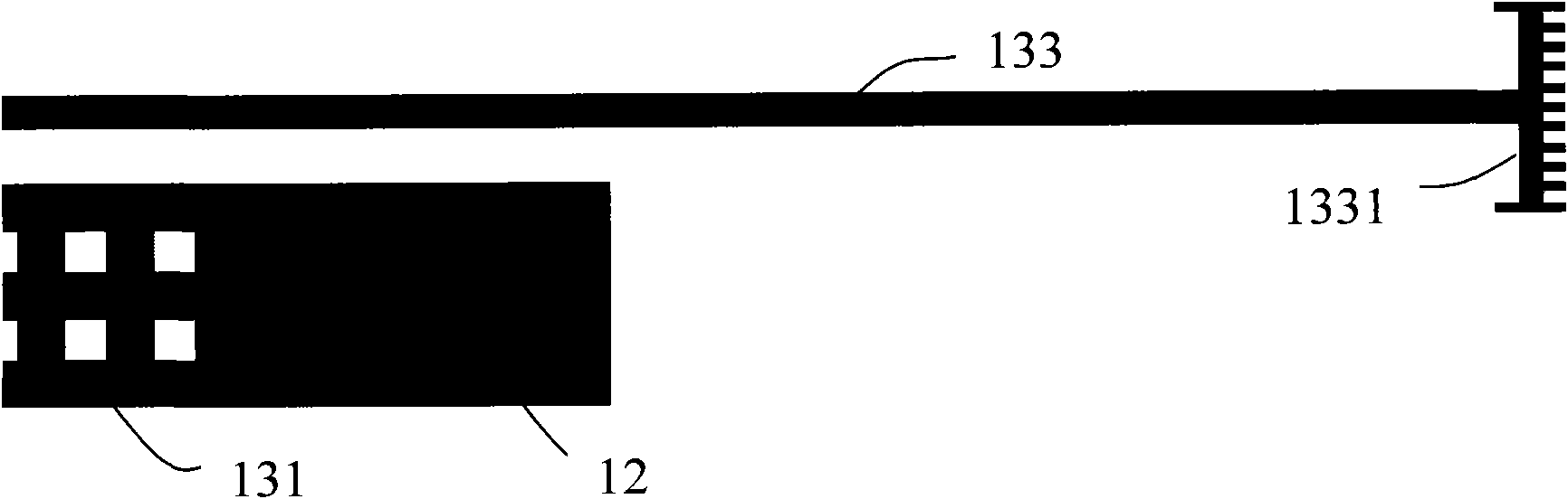
[0044] see figure 1As shown, it is a top view of the film stress test structure of the first embodiment of the present invention. The film stress test structure is arranged on the surface of the MEMS substrate, and the test structure includes: a first fixed base 11 , a second fixed base 12 , a cantilever beam 13 and a main ruler 14 . Among them, such as figure 2 As shown, the cantilever beam 13 includes: a test beam 131 , a slope beam 132 and an indicator beam 133 .

[0045] The first fixed base 11 and the second fixed base 12 are all configured on the substrate, and these two fixed bases include: a sacrificial layer formed on the substrate and a film to be measured formed on the sacrificial layer; the cantilever beam 13 is A suspended structure compo...


PUM

PropertyMeasurementUnit
thicknessaaaaaaaaaa

Abstract

The invention discloses membrane stress testing structure and method as well as a manufacturing method. The membrane stress testing structure is configured on the surface of a substrate of a micro electro mechanical system and comprises a first fixed base, a second fixed base, a cantilever beam and a main scale, wherein the first fixed base and the second fixed base are both configured on the substrate and consist of a sacrifice layer formed on the substrate and a thin film to be tested, which is formed on the sacrifice layer; the cantilever beam is in a suspended structure formed by the thin film to be tested and comprises a test beam, a slope beam and an indication beam, wherein one end of the indication beam is in a comb structure and forms a vernier; and the main scale consists of the sacrifice layer formed on the substrate and the thin film to be tested, which is formed on the sacrifice layer, and the main scale is in a comb structure configured on the substrate and used for reading the displacement of the indication beam by matching with the vernier. The membrane stress testing structure and method as well as the manufacturing method can accurately measure the membrane stress without using the Poisson ratio of materials to be tested and can also accurately measure the local region stress.

Description

technical field [0001] The invention relates to a micro-electromechanical system (MEMS) testing technology, in particular to a film stress testing structure, testing method and manufacturing method. Background technique [0002] The existing micro-electromechanical system (MEMS) is similar to the integrated circuit (IC). It also prepares a certain circuit or structure on a single crystal silicon wafer through thin film deposition, diffusion, photolithography, etching, hollowing out and other processes. Certain effects of mechanics achieve the purpose of sensing a certain signal or executing it. [0003] However, there are also differences between MEMS and traditional integrated circuits. This difference is mainly reflected in the standardization of its preparation process. The materials and processes used in integrated circuits have reached a high degree of standardization in the industry, while micro-electro-mechanical systems cannot be standardized in a short period of ti...

Claims


Application Information

Patent Timeline
Patent Type & Authority Applications(China)
IPC IPC(8): G01L1/04B81B7/02B81C5/00B81C1/00
Inventor 方辉雷述宇
Owner 北方广微科技有限公司
Why Eureka
Try Eureka