Electronic label package and manufacturing method thereof

A technology of electronic tags and production methods, which is applied in the direction of circuits, electrical components, and electrical solid devices, can solve the problems of inability to realize identification, management, tracking, and traceability, and achieve the effects of preventing damage, failure, and relieving stress

Inactive Publication Date: 2010-10-27
SHANGHAI ESTAR TECH
View PDF0 Cites 2 Cited by
  • Summary
  • Abstract
  • Description
  • Claims
  • Application Information

AI Technical Summary

Problems solved by technology

Through this packaging method, the electronic tag chip is exposed in the air. If this electronic tag and objects, such as cartons, pallets or packing boxes, go through the production process of hundreds of degrees Celsius and dozens of atmospheric pressures together, The damage rate of electronic tags is almost 100%, and the purposes of identification, management, tracking and tracing cannot be achieved at all

Method used


Image

  • Electronic label package and manufacturing method thereof
  • Electronic label package and manufacturing method thereof
  • Electronic label package and manufacturing method thereof

Examples


Embodiment Construction

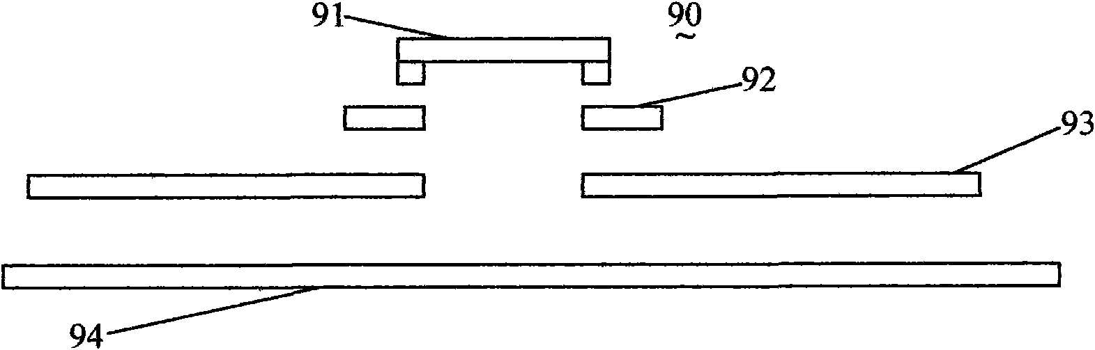
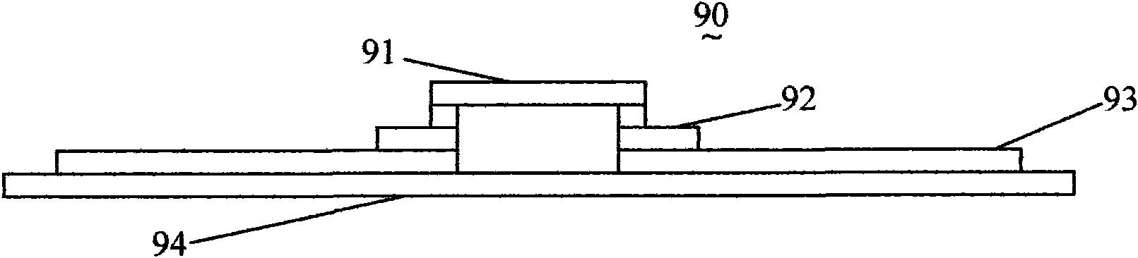
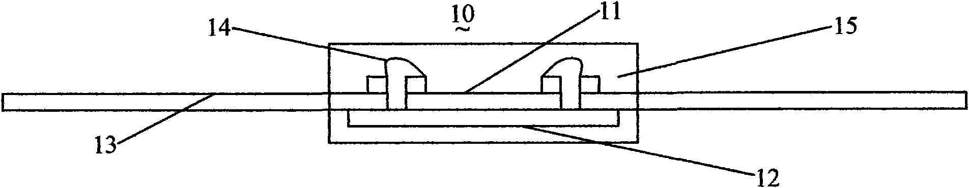
[0023] Specific embodiments of the present invention will be described in detail below in conjunction with the accompanying drawings.

[0024] The invention adopts a new packaging method, which can prevent the electronic label chip from being corroded and damaged by impurities in the air, high temperature, high pressure and moisture to the chip circuit, resulting in electrical performance degradation or failure, and the chip is completely isolated from the outside world, protecting the Protect the chip surface and connecting leads, etc., so that the very soft chip is protected from external force damage and external environment in terms of electrical or thermal physics. At the same time, the thermal expansion coefficient of the chip is matched with that of the frame or substrate through packaging, so that the stress caused by changes in the external environment such as heat and pressure can be relieved, thereby preventing chip damage and failure. Based on heat dissipation requ...


PUM


Abstract

The invention relates to an electronic label package comprising an electronic label wafer, a package pin and a substrate for placing the electronic label wafer and the package pin. The package pin is electrically connected with the electronic label wafer; besides, the electronic label wafer, the package pin, leads and the substrate are packaged in a package filling body together. The invention also provides a manufacturing method of the electronic label package, comprising the following steps of: manufacturing a wafer, and manufacturing a plurality of electronic label wafers in matrix arrangement on the wafer; cutting the wafer to obtain the separate electronic label wafer; picking up the electronic label wafer and directly placing the electronic label wafer on the substrate; manufacturing the package pin and placing the package pin on the substrate; electrically connecting the package pin with the electronic label wafer; and encapsulating the electronic label wafer, the substrate and the package pin with the package filling body.

Description

technical field [0001] The invention relates to an electronic label package, and at the same time relates to a manufacturing method of the electronic label package. Background technique [0002] Electronic tags, also known as RFID (Radio Frequency Identification) radio frequency identification, is a non-contact automatic identification technology. Through the radio waves emitted by sensors within a distance of several centimeters to several meters, the information stored in the electronic tag can be read to identify the identity of the items, people and appliances represented by the electronic tag. Like other commonly used AIDs such as barcodes and magnetic stripes, RFID is an AID technology. Each target object corresponds to a unique electronic identification code (UID) in the radio frequency card reader, which is attached to the object to identify the target object, such as a carton, pallet or packing box. The radio frequency card reader (transponder) reads the identific...

Claims


Application Information

Patent Timeline
Patent Type & Authority Applications(China)
IPC IPC(8): H01L23/48H01L23/31H01L23/29H01L21/48H01L21/50H01L21/60H01L21/56H01L21/00G06K19/07
CPCG06K19/07749H01L2224/48091
Inventor 杨军良钟卫
Owner SHANGHAI ESTAR TECH
Why Eureka
Try Eureka