Method for manufacturing ohmic contact on SiC matrix for preventing transverse spreading of metal

An ohmic contact and substrate technology, applied in semiconductor devices and other directions, can solve the problems of increasing parasitic parameters, deviating from design requirements, reducing the performance of SiC devices or circuits, and achieving the effect of reducing parasitic parameters and improving performance

Active Publication Date: 2010-11-10
THE 13TH RES INST OF CHINA ELECTRONICS TECH GRP CORP
View PDF2 Cites 2 Cited by
  • Summary
  • Abstract
  • Description
  • Claims
  • Application Information

AI Technical Summary

Problems solved by technology

Since the thermal expansion coefficients of the metal layer and the SiC substrate are different at high temperatures of 900°C to 1200°C, and the thermal expansion coefficient of the metal layer is relatively large, it will expand laterally during high-temperature annealing, which deviates from the design requirements and increases parasitic parameters, reducing the performance of SiC devices or circuits

Method used


Image

  • Method for manufacturing ohmic contact on SiC matrix for preventing transverse spreading of metal
  • Method for manufacturing ohmic contact on SiC matrix for preventing transverse spreading of metal
  • Method for manufacturing ohmic contact on SiC matrix for preventing transverse spreading of metal

Examples


Embodiment Construction

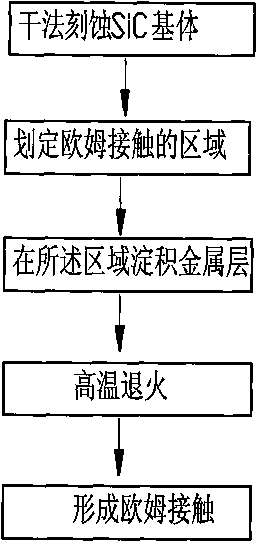
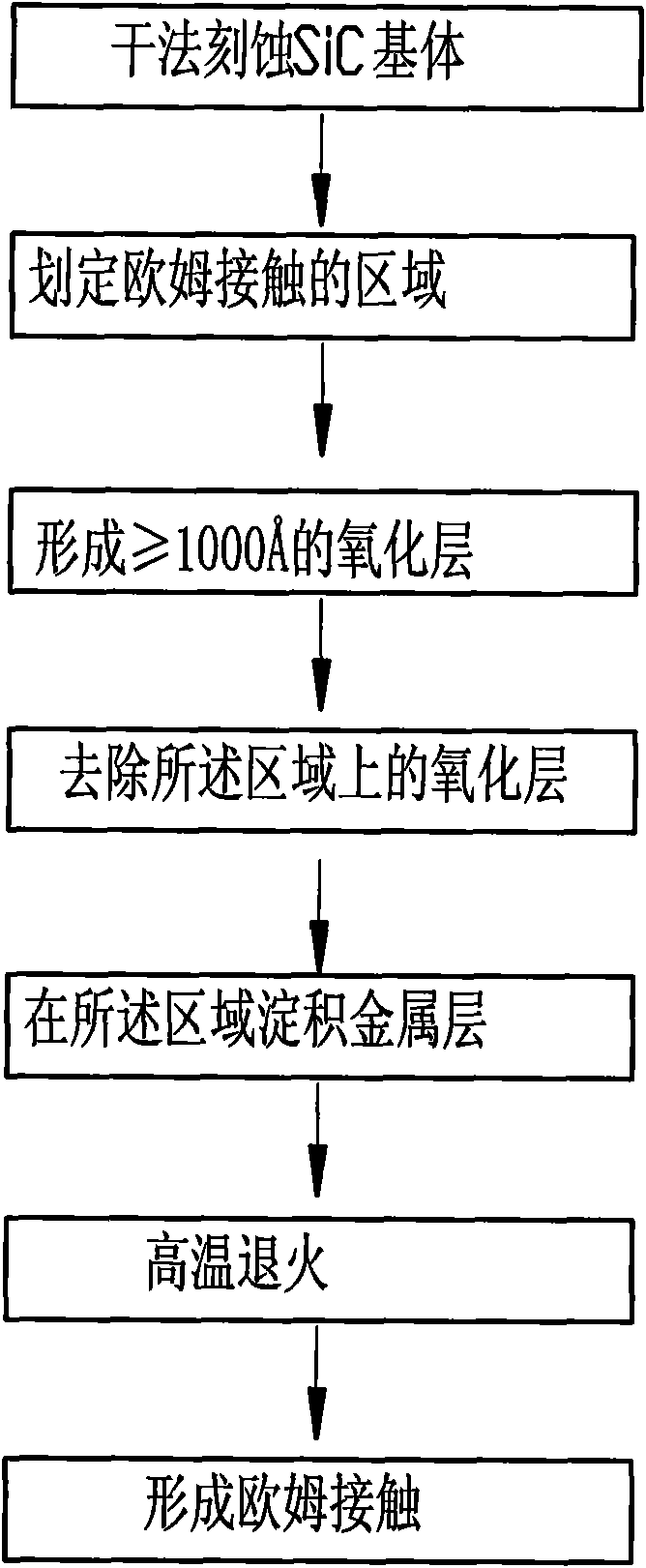
[0020] Process flow of the present invention such as figure 2 shown. Below take the ohmic contact of making field effect transistor as example, illustrate the method for making ohmic contact of the present invention:

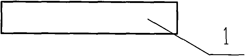
[0021] 1) The required SiC substrate 1 is etched out by dry etching method, see image 3 .

[0022] 2) On the upper surface of the SiC substrate 1, a groove 5 is etched by dry etching, and the groove 5 is used to make a Schottky contact, see Figure 4 ; Delimit the area of ​​the ohmic contact outside the groove on the SiC substrate. The dry etching is performed according to an existing process.

[0023] 3) Oxidation step: Oxidize the upper surface of the SiC substrate and its adjacent side walls to form a thickness of 1000~ oxide layer 2, see Figure 5 . The composition of the oxide layer is SiO 2 .

[0024] The conditions for the oxidation step are:

[0025] Oxidation temperature: 1200~1350℃;

[0026] Oxidation rate: ≥ / Hour;

[0027] Oxidizing ...


PUM


Abstract

The invention discloses a method for manufacturing ohmic contact on an SiC matrix for preventing transverse spreading of metal, which is characterized by consisting of the following steps of: dry-etching the SiC matrix, dividing a region for ohmic contact, depositing a metal layer in the region, and carrying out high-temperature annealing to form the ohmic contact, wherein before the step of depositing the metal layer, the following steps are added : (1) an oxidization step for oxidizing the SiC matrix to form an oxide layer with thickness of not less than 1000 angstroms; (2) and a step of removing the oxide layer on the region of the ohmic contact. By adopting the invention, the certain transverse spreading of the molten metal layer is effectively prevented in the high-temperature annealing process; a ohmic electrode is manufactured conveniently according to the design requirements; parasitical parameters are reduced and the performance of the SiC device or the circuit is improved.

Description

technical field [0001] The invention belongs to the technical field of making electrodes on semiconductor materials, and in particular relates to a method for preventing lateral expansion of metal layers when making ohmic contacts on SiC devices. Background technique [0002] SiC is a rapidly developing semiconductor material, known as the "third-generation semiconductor" after silicon and gallium arsenide, and has broad prospects in the preparation of semiconductor devices. [0003] In order to effectively connect the SiC device to the outside, it is necessary to make a contact between the SiC device and the metal wiring. There are two types of contacts that are frequently used: ohmic contacts and rectifying contacts. In an ideal ohmic contact, the current varies linearly with the applied voltage. In order to transmit as much current as possible from the SiC device to the entire circuit, the ratio of the ohmic contact resistance to the entire device resistance must be sma...

Claims


Application Information

Patent Timeline
Patent Type & Authority Applications(China)
IPC IPC(8): H01L21/28
Inventor 霍玉柱潘宏菽商庆杰齐国虎
Owner THE 13TH RES INST OF CHINA ELECTRONICS TECH GRP CORP
Why Eureka
Try Eureka