
Manufacturing method of phase-changing random access memory

A technology for accessing memory and manufacturing methods, which is applied in semiconductor/solid-state device manufacturing, electrical components, circuits, etc. It can solve the problems of device quality degradation, dielectric layer and polysilicon column loss, etc., and achieve the effect of overcoming short circuit

Inactive Publication Date: 2012-08-22
SEMICON MFG INT (SHANGHAI) CORP +1
View PDF7 Cites 0 Cited by
  • Summary
  • Abstract
  • Description
  • Claims
  • Application Information

AI Technical Summary

Problems solved by technology

[0006] However, in the prior art, the core structure of the phase change random access memory is integrated with the decoding circuit and the peripheral MOS circuit, and some metal plugs used in the manufacture of the decoding circuit and the peripheral MOS circuit cannot be avoided when manufacturing the core structure. remains on the sidewall of the plug hole, causing a short circuit
[0007] In addition, when manufacturing decoding circuits and peripheral MOS circuits, during the process of removing metal plugs, the loss of dielectric layers and polysilicon pillars is too much, resulting in a decline in the quality of the manufactured devices

Method used


Image

  • Manufacturing method of phase-changing random access memory
  • Manufacturing method of phase-changing random access memory
  • Manufacturing method of phase-changing random access memory

Examples


Embodiment Construction

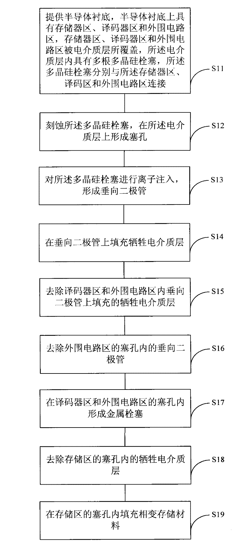
[0028] In one embodiment of the present invention, a method for manufacturing a phase change random access memory is provided, such as figure 2 shown, including steps:

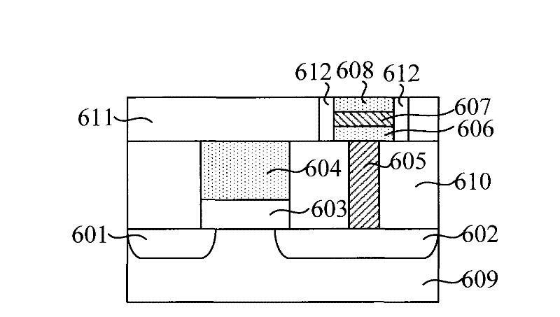
[0029] S11, providing a semiconductor substrate, the semiconductor substrate has a memory area, a decoder area and a peripheral circuit area, the memory area, the decoder area and the peripheral circuit area are covered by a dielectric layer, and the dielectric layer has a plurality of polysilicon a plug, the polysilicon plug is respectively connected to the memory area, the decoding area and the peripheral circuit area;

[0030] S12, etching the polysilicon plug to form plug holes on the dielectric layer;

[0031] S13, performing ion implantation on the polysilicon plug to form a vertical diode;

[0032] S14, filling the sacrificial dielectric layer on the vertical diode;

[0033] S15, removing the sacrificial dielectric layer filled on the vertical diodes in the decoder area and the peripheral circuit ar...


PUM


Abstract

The invention relates to a manufacturing method of a phase-changing random access memory, comprising the following steps: providing a semiconductor substrate at least provided with a memory region, a peripheral circuit region and a plurality of polysilicon plugs connected with the memory region and the peripheral circuit region; etching the polysilicon plugs; performing ion implantation to the polysilicon plugs; filling a sacrifice electrolyte layer on a vertical diode; removing the sacrifice electrolyte layer filled on the vertical diode in the peripheral circuit region; removing the vertical diode of the peripheral circuit region; forming metallic plugs in plug holes of the peripheral circuit region; removing the sacrifice electrolyte layer in the plug holes in the memory region; and filling the phase-changing memory material in the plug holes in the memory region. Compared with the prior art, the plug hole in the memory region are filled by the sacrifice electrolyte layer, so, in the manufacturing process of the device, the metallic plugs cannot form in the plug holes in the memory region, thereby conquering the problem of short circuit. etc caused by the residual metal when removing the metallic plugs in the plug holes in the memory region.

Description

technical field [0001] The present invention relates to the field of semiconductor manufacturing, in particular to a manufacturing method of a phase change random access memory. Background technique [0002] Phase Change Random Access Memory (Phase Change RAM, PCRAM) is a new type of memory that replaces NAND Flash. In phase change random access memory, the phase change layer in which data is recorded can be heat treated to change the value of the memory. The phase-change material constituting the phase-change layer may enter a crystalline state or an amorphous state due to the heating effect of the applied current. When the phase change layer is in a crystalline state, the resistance of the PCRAM is low, and the memory is assigned a value of "0" at this time. When the phase change layer is in an amorphous state, the resistance of the PCRAM is high, and the memory is assigned a value of "1" at this time. Therefore, the PCRAM is a nonvolatile memory that writes / reads data ...

Claims


Application Information

Patent Timeline
Patent Type & Authority Patents(China)
IPC IPC(8): H01L21/8229H01L21/306H01L21/311H01L21/20
Inventor 洪中山何其旸
Owner SEMICON MFG INT (SHANGHAI) CORP
Learn More