
Light trap adopted epitaxial material structure of ultrafine divergent angle high-power semiconductor laser

A technology of epitaxial materials and optical traps, applied in the direction of semiconductor lasers, lasers, laser components, etc., can solve the problems of poor device spot symmetry, unfavorable laser beam efficient coupling, etc., and achieve the effect of reducing the vertical divergence angle of the far field

Inactive Publication Date: 2010-11-17
INST OF SEMICONDUCTORS - CHINESE ACAD OF SCI
View PDF0 Cites 12 Cited by
  • Summary
  • Abstract
  • Description
  • Claims
  • Application Information

AI Technical Summary

Problems solved by technology

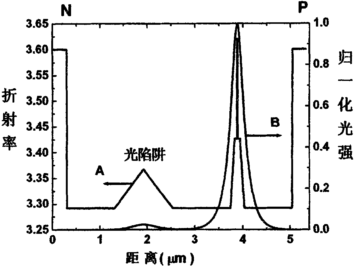
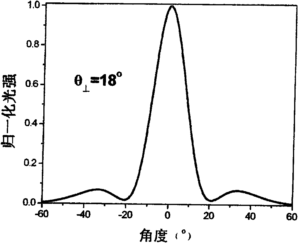
At present, the far-field vertical divergence angle and parallel divergence angle of ordinary waveguide structure high-power semiconductor lasers are too different, and the typical value is 40° (vertical divergence angle, θ ⊥ )×10°(parallel divergence angle, θ / / ), so the symmetry of the device spot is extremely poor, which is not conducive to the efficient coupling of the laser beam and the pumped device

Method used


Image

  • Light trap adopted epitaxial material structure of ultrafine divergent angle high-power semiconductor laser
  • Light trap adopted epitaxial material structure of ultrafine divergent angle high-power semiconductor laser
  • Light trap adopted epitaxial material structure of ultrafine divergent angle high-power semiconductor laser

Examples


Embodiment Construction

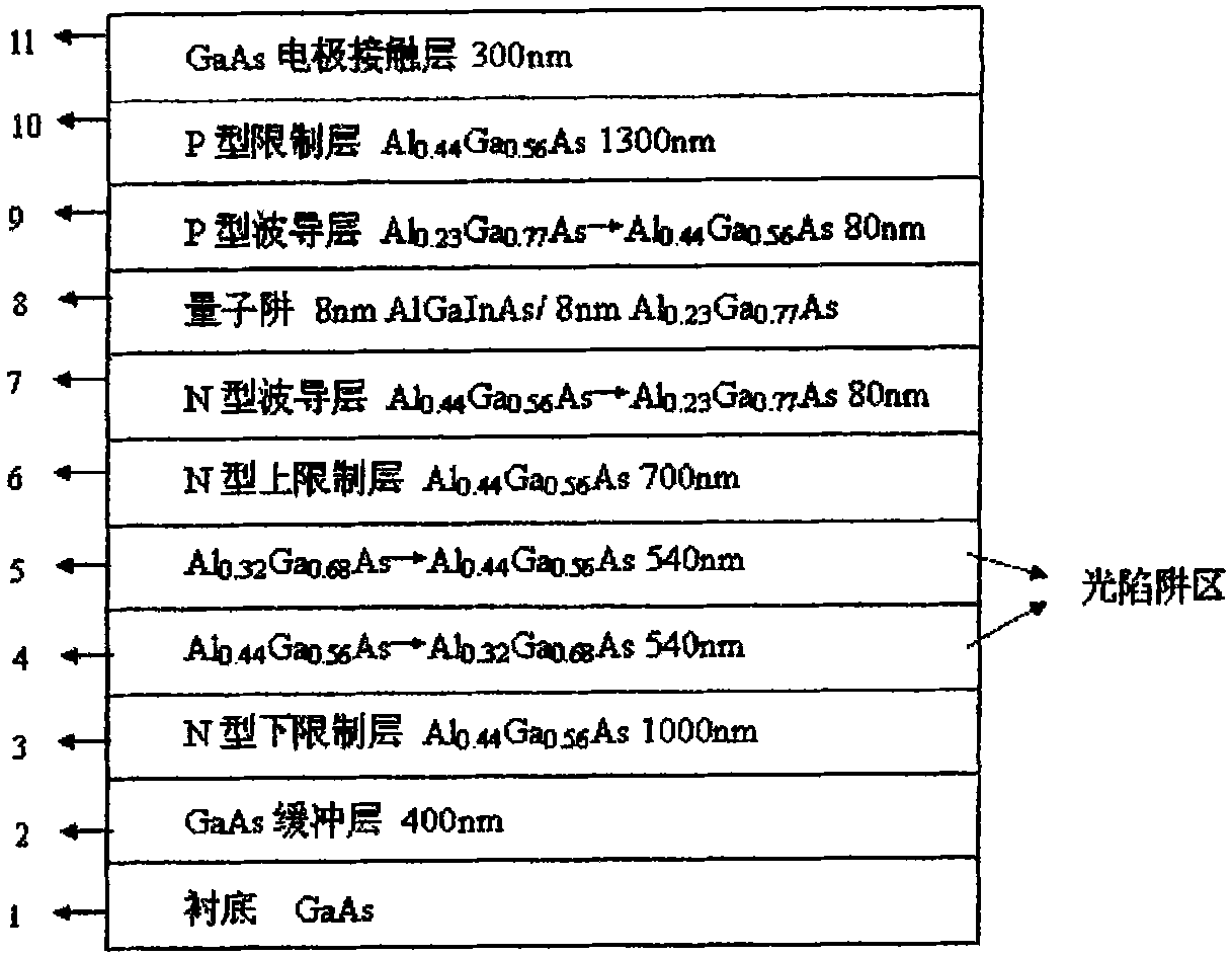
[0034] see figure 1 As shown, the present invention adopts an optical trap ultra-small divergence angle high-power semiconductor laser epitaxial material structure, which is characterized in that it includes:

[0035] A substrate 1, the GaAs substrate 1 is used to carry out the epitaxial growth of each layer of the laser material thereon, the substrate is an N-type GaAs material of the (100) plane, and the Si doping concentration is 1-2×10 18 cm -3 , with a thickness of 320-380 μm;

[0036] A buffer layer 2, which is made on the GaAs substrate 1, is N-GaAs material, and the Si doping concentration is 1-2×10 18 cm -3 , the thickness is 300-600nm;

[0037] An N-type lower confinement layer 3, the N-type lower confinement layer 3 is made on the buffer layer 2, and the N-type lower confinement layer 3 is N-Al 0.44 Ga0.56 As material, Si doping concentration is 1-2×10 18 cm -3 , the thickness is 1000-1200nm;

[0038] A graded optical trap layer 4, which is fabricated on the...


PUM

PropertyMeasurementUnit
Thicknessaaaaaaaaaa
Thicknessaaaaaaaaaa
Thicknessaaaaaaaaaa

Abstract

The invention relates to a light trap adopted epitaxial material structure of an ultrafine divergent angle high-power semiconductor laser, which comprises a substrate, a buffer layer, an N-type lower limiting layer, a lower gradient light trap layer, an upper gradient light trap layer, an N-type upper limiting layer, an N-type gradient waveguide layer, a quantum well active area, a P-type gradient waveguide layer, a P-type limiting layer and an electrode contact layer, wherein the substrate is used for carrying out the epitaxial growth of all layers of materials of a laser; the buffer layer is prepared on the GaAs substrate; the N-type lower limiting layer is prepared on the buffer layer; the lower gradient light trap layer is prepared on the N-type lower limiting layer; the upper gradient light trap layer is prepared on the lower gradient light trap layer; the N-type upper limiting layer is prepared on the lower gradient light trap layer; the N-type gradient waveguide layer is prepared on the N-type lower limiting layer; the quantum well active area is prepared on the N-type gradient waveguide layer; the P-type gradient waveguide layer is prepared on the quantum well active area; the P-type limiting layer is prepared on the P-type gradient waveguide layer; and the electrode contact layer is prepared on the P-type limiting layer.

Description

technical field [0001] The invention relates to an epitaxial material structure of a high-power semiconductor laser, in particular to an epitaxial material structure of a high-power semiconductor laser with a wavelength of 885nm that can improve the pumping efficiency of an all-solid-state laser and has a very low beam vertical divergence angle. Background technique [0002] High-power semiconductor lasers have the advantages of high electro-optical efficiency, small size, light weight and long life, so they have important applications in the fields of industry, military, aviation, medical treatment and space communication. Especially in recent years, high-power semiconductor lasers with a wavelength range of 800nm-980nm and their arrays have become necessary pumping sources for high-energy solid-state lasers and fiber lasers. [0003] For all-solid-state lasers, the main limitation of high power and high beam quality comes from the huge useless heat generated during the pum...

Claims


Application Information

Patent Timeline
IPC IPC(8): H01S5/00H01S5/343H01S5/028
Inventor 王俊白一鸣崇锋熊聪仲莉韩淋王翠鸾冯小明刘媛媛刘素平马骁宇
Owner INST OF SEMICONDUCTORS - CHINESE ACAD OF SCI
Learn More