Photovoltaic cells having metal wrap through and improved passivation

A photovoltaic and passivation layer technology, applied in the direction of photovoltaic power generation, circuits, electrical components, etc., can solve the problems of MWT solar energy efficiency limitations, achieve the effect of reducing recombination current and improving efficiency

Inactive Publication Date: 2010-11-17
INTERUNIVERSITAIR MICRO ELECTRONICS CENT (IMEC VZW)
View PDF5 Cites 24 Cited by
  • Summary
  • Abstract
  • Description
  • Claims
  • Application Information

AI Technical Summary

Problems solved by technology

[0009] Despite the reduced shading area of ​​these MWT solar cells, the efficiency of these MWT solar cells is still generally limited due to excessive shunting that can occur, such as recombination in the vias and under the back-emitter busbars (see e.g. From the literature: "Processing and comprehensive characterization of screen-printed MC-Si Metal Wrap Through (MWT) Solar cel

Method used


Image

  • Photovoltaic cells having metal wrap through and improved passivation
  • Photovoltaic cells having metal wrap through and improved passivation
  • Photovoltaic cells having metal wrap through and improved passivation

Examples


Embodiment Construction

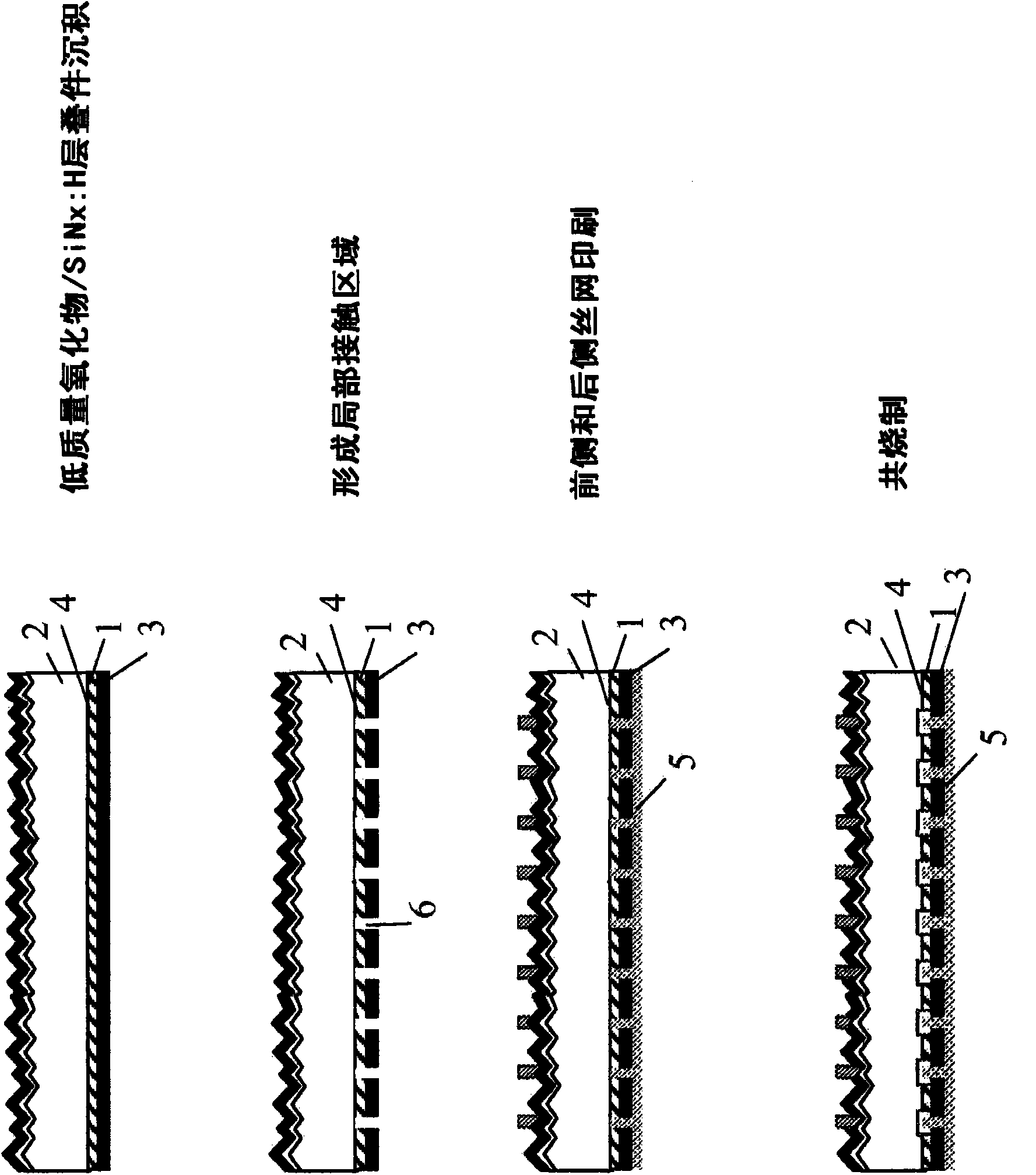
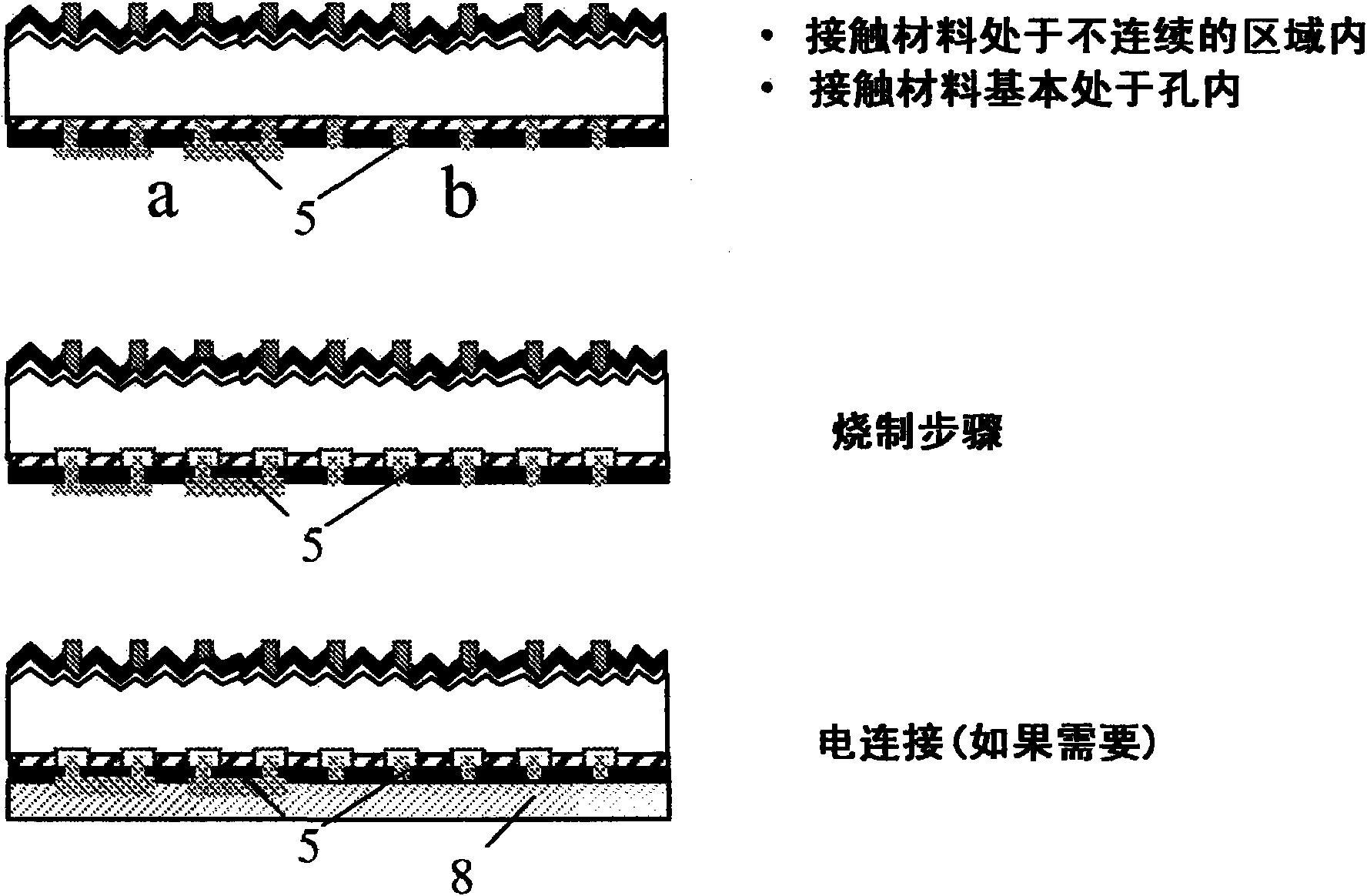
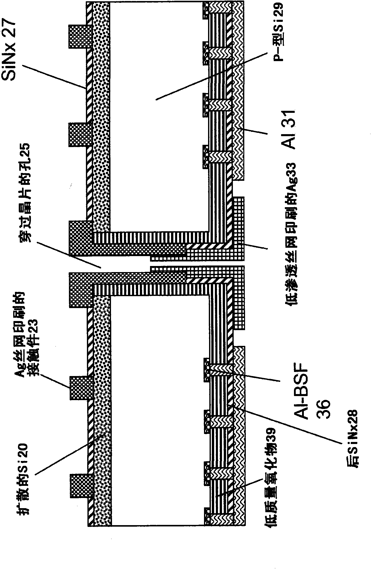
[0026] How to implement the present invention will be described below with respect to specific embodiments with reference to certain drawings, but the present invention is not limited thereto. The drawings described are only schematic and not restrictive. In the drawings, the size of some of the elements is exaggerated and not drawn on scale for illustrative purposes.

[0027] In addition, in the description as well as in the claims, the terms "first", "second" and "third" etc. are used to distinguish similar elements and do not necessarily describe a sequence or chronological order. It is to be understood that the terms are used interchangeably under appropriate circumstances and that the embodiments of the invention described herein are capable of operation in other sequences than described or illustrated herein.

[0028] In addition, in the specification and claims, the terms "top", "bottom", "above", "below" and the like are used for description and not necessarily for de...


PUM

PropertyMeasurementUnit
Thicknessaaaaaaaaaa

Abstract

A photovoltaic device in a semiconductor substrate, has a radiation receiving front surface and a rear surface, a first region of one conductivity type (29), and a second region with the opposite conductivity type (20) adjacent to the front surface, and an antireflection layer (27). The rear surface is covered by a dielectric layer (39) covering also an inside surface of the via. The front surface has current collecting conductive contacts (23) and the rear surface has conductive contacts (31) extending through the said dielectric. A conductive path is provided in the via for photogenerated current from the front surface. By having the dielectric all over, no aligning and masking is needed, and the same dielectric serves to insulate, provide thermal protection for the semiconductor, and helps in surface and bulk passivation. It also avoids the need for a junction region near the via, hence reducing unwanted recombination currents.

Description

technical field [0001] The present invention relates to photovoltaic devices such as solar cells. More specifically, the present invention relates to metal wrap through solar cells improved by special passivation schemes, and also to cost-effective methods for manufacturing said solar cells. Background technique [0002] According to the general structure, most of the solar cells described in the prior art can be divided into several categories. [0003] One class of these is the so-called back-contact solar cells, which means that the ohmic contacts to the two oppositely doped regions of the solar cell are both provided on the back side of the solar cell, ie on the non-irradiated surface. This principle avoids or reduces shading losses caused by front metal contact grids on standard solar cells. [0004] The most straightforward way to fabricate a back-contact solar cell is to place the carrier-collecting junction between oppositely doped semiconductor regions close to th...

Claims


Application Information

Patent Timeline
IPC IPC(8): H01L31/0224
CPCH01L31/1804Y02E10/50H01L31/02245Y02E10/547Y02P70/50H01L31/022441H01L31/022425H01L31/0224
Inventor F·德罗斯C·阿尔贝J·什勒夫奇克G·博卡恩
Owner INTERUNIVERSITAIR MICRO ELECTRONICS CENT (IMEC VZW)
Why Eureka
Try Eureka