Self-adaptive current mirror

A current mirror, self-adaptive technology, applied in the direction of adjusting electrical variables, control/regulating systems, instruments, etc., can solve the problems of low current accuracy and small output current range, to expand the current range, reduce costs, and reduce chip area. and the effect of complexity

Active Publication Date: 2010-11-24
苏州日月成科技有限公司
View PDF6 Cites 18 Cited by
  • Summary
  • Abstract
  • Description
  • Claims
  • Application Information

AI Technical Summary

Problems solved by technology

[0052] The present invention aims at the shortcoming that the output current range of the existing current mirror is small, and the current accuracy in the whole range is not high when the output current range is large, and provides an adaptive current mirror, which maintains a higher current range in a larger current range. Constant current accuracy

Method used


Image

  • Self-adaptive current mirror
  • Self-adaptive current mirror
  • Self-adaptive current mirror

Examples


Embodiment 1

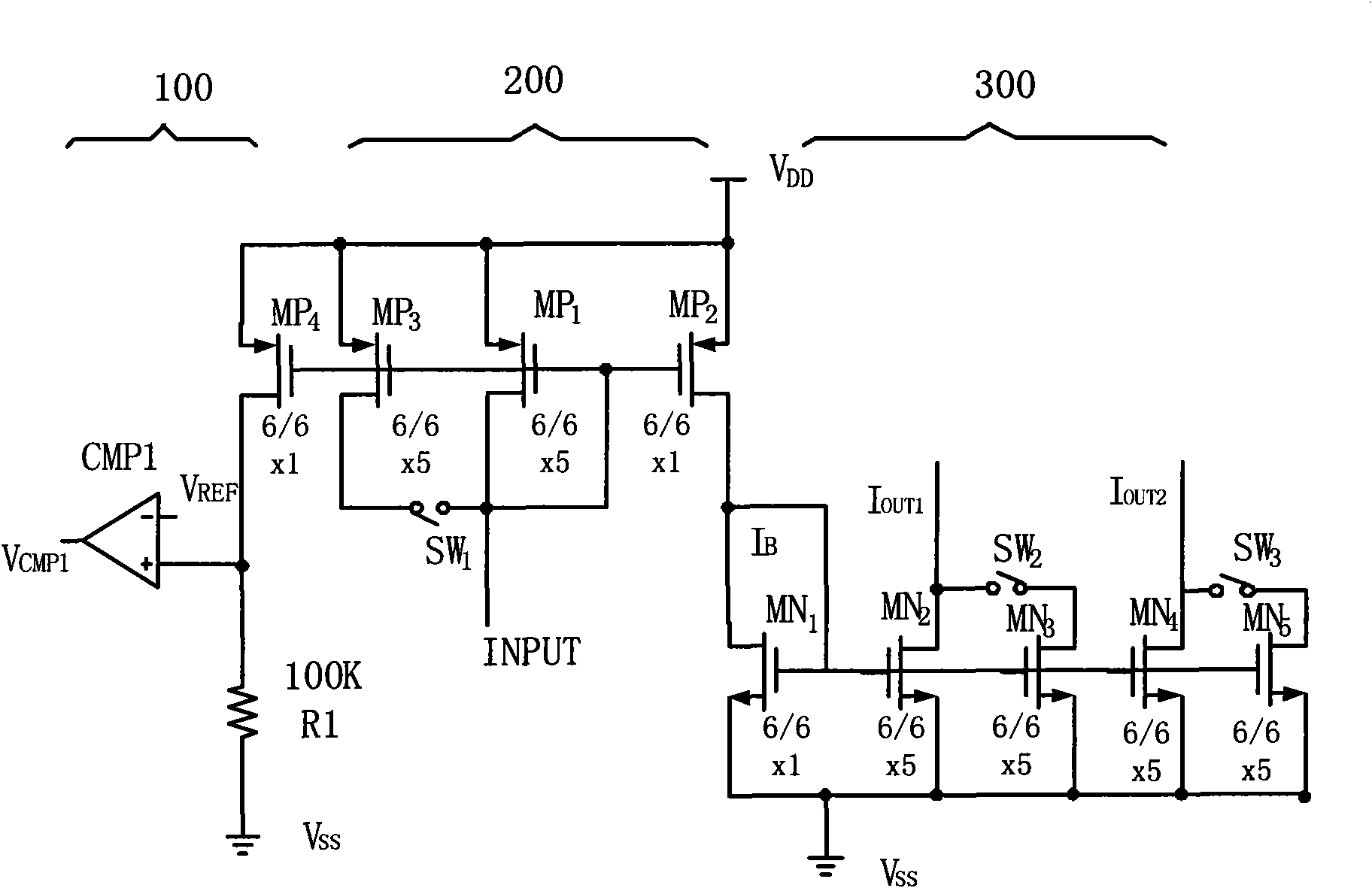
[0081] This example Image 6 As shown, it includes an input circuit unit 11 , two output circuit units 12 , 13 , two negative feedback impedance adjustment units 14 , 15 and a voltage detection and control unit 16 .

[0082] The input circuit unit 11 is composed of four NMOS transistors M11, M12, M13, M14 and three switches SW1, SW2, SW3. The gates of the four NMOS transistors are all connected to the output terminal of the operational amplifier AMP1, and the sources are all grounded. The drain of M11 is directly connected to the positive input terminal of the operational amplifier AMP1 and the input current I ref connection, NMOS tubes M12, M13, and M14 are used as alternative tubes, and their drains are connected to the positive input terminal of the operational amplifier AMP1 and the input current I through the switches SW1, SW2, and SW3 respectively. ref Connection, the negative input terminal of the operational amplifier AMP1 is connected to the reference voltage V ref ...

Embodiment 2

[0141] This example Figure 7As shown, this embodiment consists of two stages of current mirrors connected in series. Modules 100P, 200P, and 300P form a first-stage current mirror, and modules 100N, 200N, and 300N form a second-stage current mirror. The structure of the first-stage current mirror is basically the same as that of Embodiment 1, but the number of alternative transistors is reduced to two, the number of NAND gates and RS flip-flops is reduced by one each, and the MOS transistors are all PMOS transistors.

[0142] In this embodiment, the input circuit unit of the first stage current mirror is composed of P5, P6 and P7, and P6 and P7 are optional tubes. The output circuit unit of the first-stage current mirror is composed of P1, P2, and P3, and P2 and P3 are optional tubes. Due to the characteristics of the PMOS tube, the input current is a pull current, and the corresponding output current is also a pull current. The output current is the drain current of the P...

Embodiment 3

[0151] Such as Figure 8 As shown, the circuit structure of this embodiment is similar to that of Embodiment 1, but the structure is simpler, including an input circuit unit 11 , an output circuit unit 12 , a voltage detection and control unit 13 and a negative feedback impedance adjustment unit 14 . The input circuit unit 11 is composed of a basic transistor M11, an optional transistor M12 and a switch SW1 connected between the drains of the two NMOS transistors; the output circuit unit 12 is composed of a basic transistor M21, an optional transistor M22 and a connection A switch SW2 is formed between the drains of the two NMOS transistors. The structure and electrical connection of the negative feedback impedance adjustment unit 14 are the same as those in the first embodiment. Since there is only one optional tube in the input circuit unit 11 and the output circuit unit 12, correspondingly, the control of the switch is relatively simple. The state of both switches is the ...


PUM


Abstract

The invention discloses a self-adaptive current mirror, which is composed of a plurality of sub current mirrors which are connected in series, wherein each sub current mirror comprises an input circuit unit, a plurality of output circuit units, a voltage detection and control unit and a negative feedback impedance regulating unit. The input circuit unit and the output circuit unit are formed by connecting a basic transistor and a standby transistor in parallel, a switch is arranged between the basic transistor and the standby transistor, the transistors are of the same type, have the save threshold voltage and both work in a linear area. The voltage detection and control unit detects the grid voltages of the transistors in the input circuit unit and the output circuit unit, compares the grid voltages with two preset voltage references, controls the on and off of the switch according to the result of the comparison, and controls the on and off of the standby transistor for regulating the range of an output current. In the invention, the range of the output current of the conventional current mirror is expanded, and a high constant current precision is kept within a wide range of the output current.

Description

technical field [0001] The invention relates to the technical field of integrated circuits, in particular to an adaptive current mirror. Background technique [0002] In the existing multi-bit output LED constant current drive circuit, the output current is determined by the input current generated by an external resistor, and the output current and accuracy depend on the proportional current mirror. In actual use, depending on the specific application, the required output current will be different. However, the working range of the current mirror in the prior art is limited, especially the working range for maintaining high precision is limited. In order to meet different output current requirements, the usual practice is to design and produce multiple chip products according to different current ranges, or to provide different accuracy ranges on the same chip. For example, currently on the market with an on-chip accuracy of ±3% common 3-45mA range, 10-50mA range, 20-30mA...

Claims


Application Information

Patent Timeline
Patent Type & Authority Applications(China)
IPC IPC(8): G05F3/26
Inventor 赵一尘卢晓冬唐仁明何乐年
Owner 苏州日月成科技有限公司
Why Eureka
Try Eureka