P-type one-time programmable (OTP) device and manufacturing method thereof

A manufacturing method and device technology, applied in semiconductor/solid-state device manufacturing, electric solid-state devices, semiconductor devices, etc., can solve the problems of low reading current, large chip area, and small current value, so as to improve the conduction current, The effect of improved programming performance and increased coupling capacitance

Active Publication Date: 2015-06-03
SHANGHAI HUAHONG GRACE SEMICON MFG CORP
View PDF3 Cites 0 Cited by
  • Summary
  • Abstract
  • Description
  • Claims
  • Application Information

AI Technical Summary

Problems solved by technology

This will consume a lot of OTP peripheral circuit area
Although the unit area of ​​each P-type OTP device is very small, more peripheral circuits limit the application of this type of device to applications that require high-density capacity
[0007] like Image 6 As shown, it is the working curve before and after programming of the existing P-type OTP device with 1V substrate bias voltage; the distinguishable current range of the device before and after programming becomes larger, but the current value before and after programming becomes smaller
When the substrate voltage is too high, the reading current will be too low, and the reading circuit cannot read the current of the programmed OTP unit; if the substrate voltage is too low, the initial current of the OTP unit before programming is too large, and it cannot be distinguished Status of the OTP unit
Therefore, it usually requires a very complicated peripheral reading circuit to provide two accurate voltages to the substrate and the source at the same time, which consumes a large chip area at the same time.

Method used


Image

  • P-type one-time programmable (OTP) device and manufacturing method thereof
  • P-type one-time programmable (OTP) device and manufacturing method thereof
  • P-type one-time programmable (OTP) device and manufacturing method thereof

Examples


Embodiment Construction

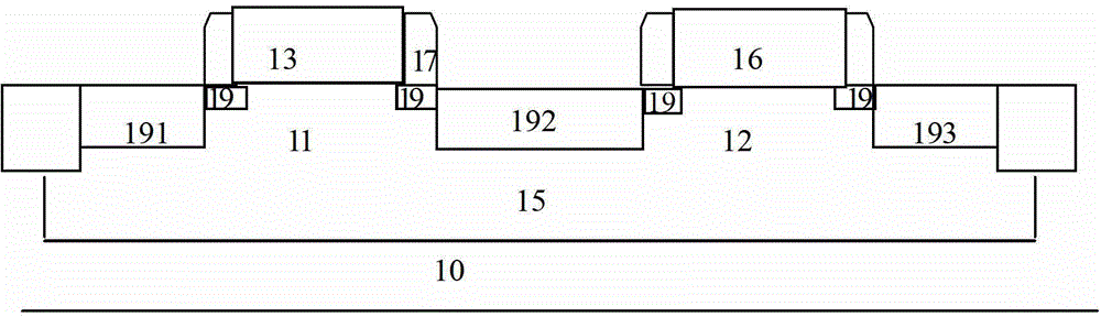
[0036] Such as figure 2 As shown, it is a schematic diagram of the structure of a P-type OTP device according to an embodiment of the present invention. An N-type well 15 is formed on a silicon substrate 10, and a one-time programmable device formed by connecting two PMOS transistors 11 and 12 in series. The first PMOS The transistor 11 is used as a pass transistor of the OTP device, and the second PMOS transistor 12 is used as a storage unit of the OTP device.

[0037] The source of the first PMOS transistor 11 includes a P-type diffusion region 191 and a P-type lightly doped region 19 formed in the N well, and the drain of the first PMOS transistor 11 includes a P-type diffused region 191 formed in the N well. A P-type diffusion region 192 and a P-type lightly doped region 19, the gate 17 of the first PMOS transistor is used as the word line of the OTP device, and the source of the first PMOS transistor 11 is used as the word line of the OTP device. Source of the OTP devic...


PUM


Abstract

The invention discloses a P-type OTP device. A source of a second P-channel metal oxide semiconductor (PMOS) transistor of the P-type OTP device comprises a first P-type foreign ion implantation region, the first P-type foreign ion implantation region extends from an edge position of a P-type diffusion region of the second PMOS transistor to the bottom of a gate of the second PMOS transistor and forms a first coupling region between the source of the second PMOS transistor and the grid of the second PMOS transistor, the width of the first coupling region is wider than those of second coupling regions formed by all P-type lightly-doped regions and corresponding grids, and the concentration of the first coupling region is greater than those of second coupling regions. The invention also discloses a manufacturing method of the P-type OTP device. By the aid of the P-type OTP device and the manufacturing method, the programming performance of the P-type OTP device can be greatly improved, the breakover current of the whole device after programming is improved, current ranges which can be distinguished before and after programming of the device can be increased, and the area of a peripheral circuit which is used for implementing an OTP function can be reduced.

Description

technical field [0001] The invention relates to the field of manufacturing semiconductor integrated circuits, in particular to a P-type OTP device, and also relates to a method for manufacturing the P-type OTP device. Background technique [0002] Such as figure 1 As shown, it is a schematic diagram of the structure of the existing P-type OTP device. An N-type well 15 is formed on the silicon substrate 10. It is a one-time programmable device formed by connecting two PMOS transistors 11 and 12 in series. The first PMOS transistor 11 serves as The gate transistor of the OTP device, and the second PMOS transistor 12 is used as the storage unit of the OTP device. [0003] The source of the first PMOS transistor 11 includes a P-type diffusion region 191 and a P-type lightly doped region 19 formed in the N well, and the drain of the first PMOS transistor 11 includes a P-type diffused region 191 formed in the N well. A P-type diffusion region 192 and a P-type lightly doped regio...

Claims


Application Information

Patent Timeline
Patent Type & Authority Patents(China)
IPC IPC(8): H01L27/115H01L21/8247
Inventor 黄景丰胡晓明刘梅
Owner SHANGHAI HUAHONG GRACE SEMICON MFG CORP
Why Eureka
Try Eureka