Multilayer substrate including GaN layer, method for manufacturing the multilayer substrate including GaN layer, and device
A technology for stacking substrates and manufacturing methods, which is applied in the fields of semiconductor devices, chemical instruments and methods, semiconductor/solid-state device manufacturing, etc., can solve the problems of high price and difficult to obtain, and achieve the effect of low cost
- Summary
- Abstract
- Description
- Claims
- Application Information
AI Technical Summary
Problems solved by technology
Method used
Image
Examples
Embodiment 1
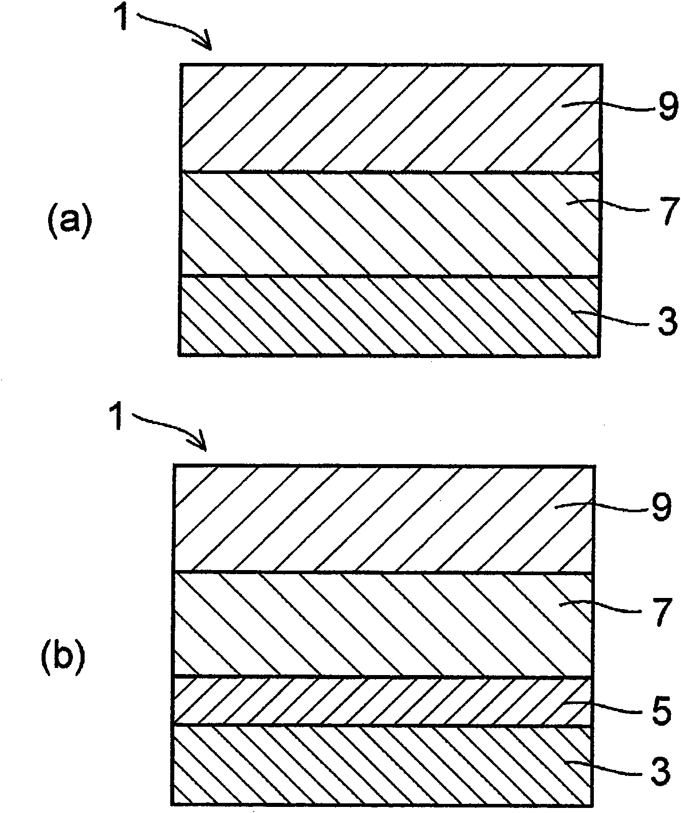
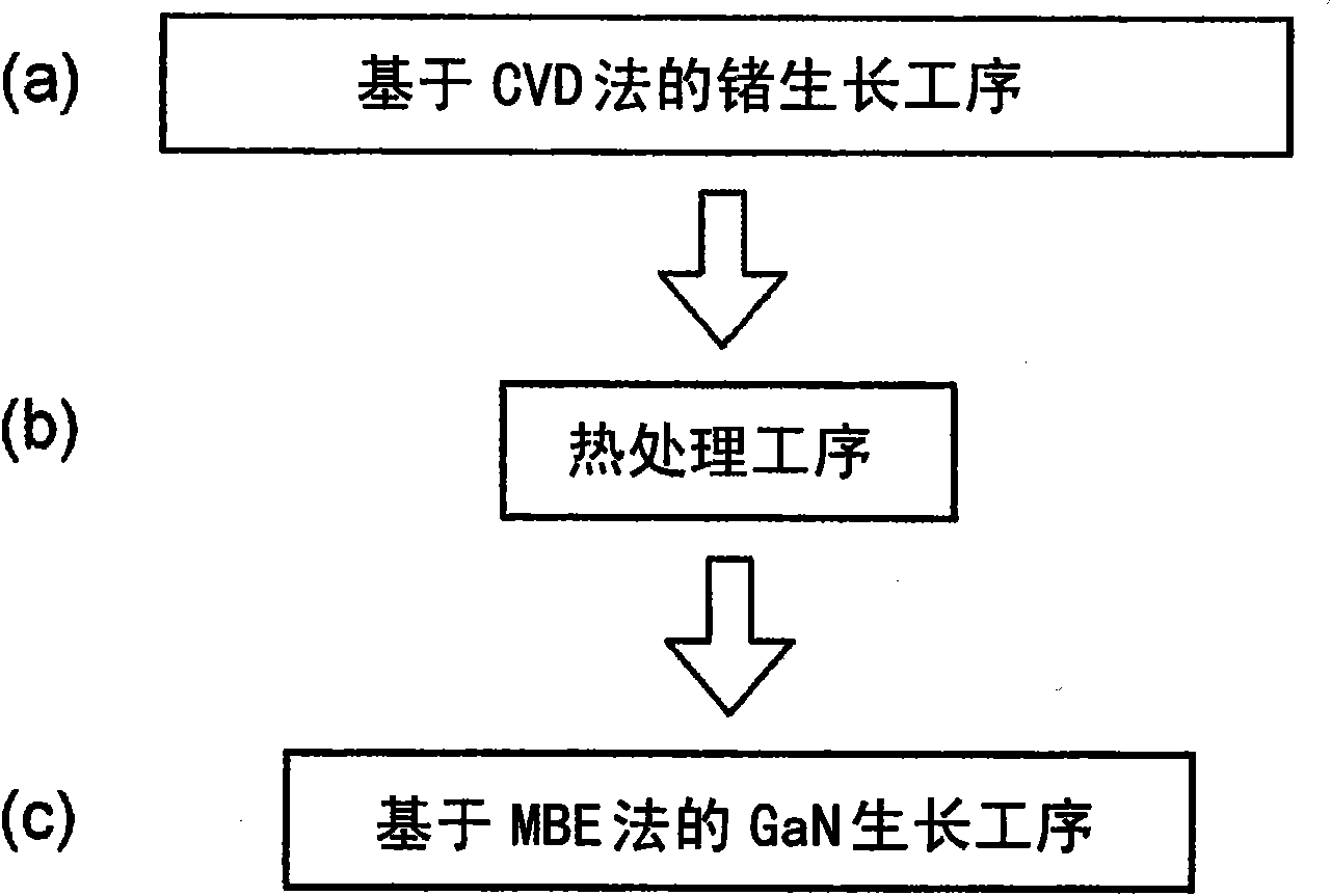
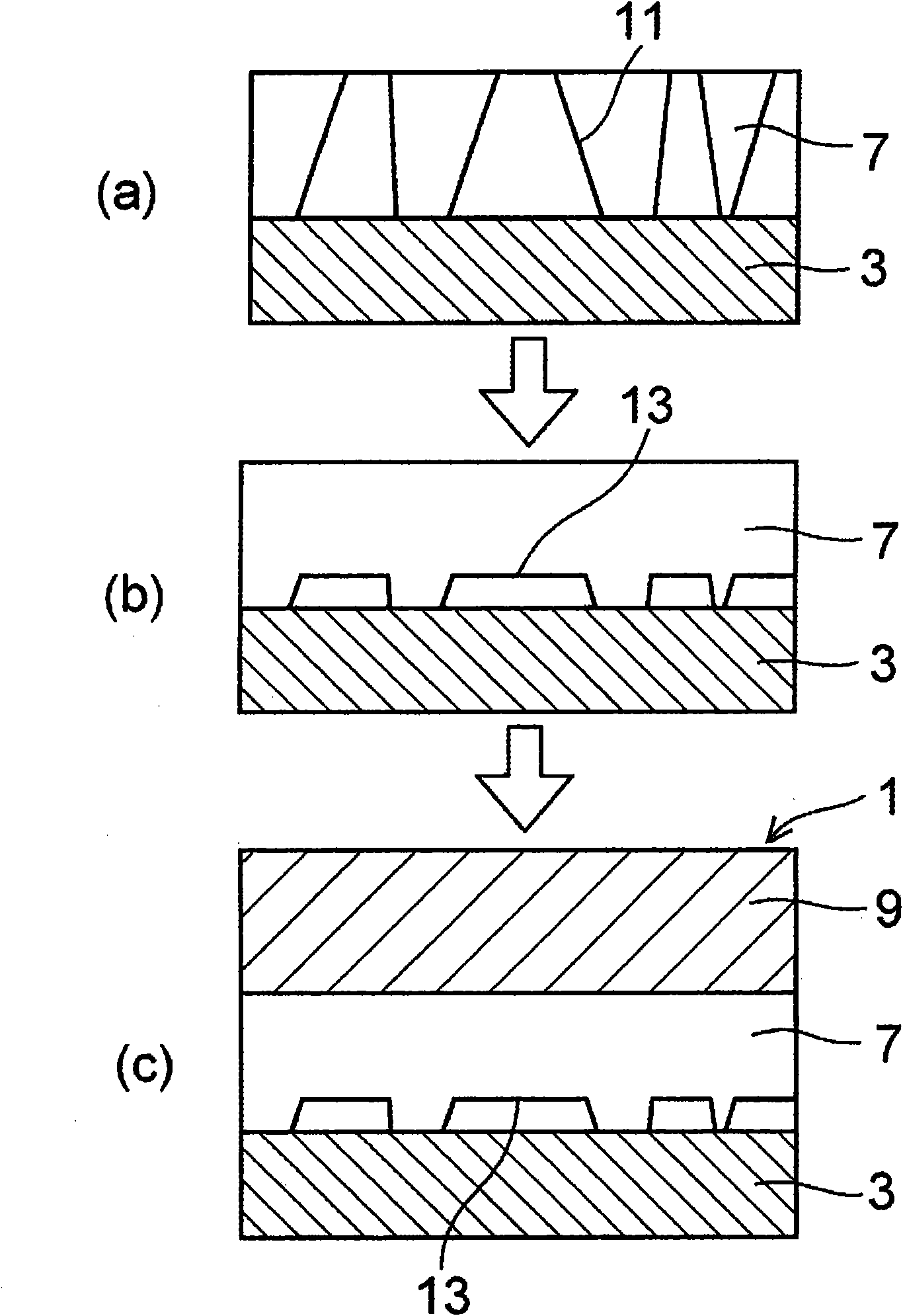
[0055] (111) germanium is epitaxially grown directly on (111) silicon substrate by chemical vapor deposition method (CVD method) so that the thickness on silicon is about 100 nm, and heat treatment is performed at 800°C. Subsequently, GaN was grown by the MBE method to obtain a GaN film of about 50 nm. When this GaN film was analyzed by X-ray diffraction, a sharp peak at about 380 arcsec was observed, and it was confirmed that a GaN single crystal was growing.
[0056] When the cross-section of the obtained laminated substrate including the GaN layer was observed by TEM (Transmission Electron Microcopy), threading dislocations were not observed in the germanium layer, but dislocations locally existed near the interface between the silicon substrate and the germanium layer.
Embodiment 2
[0058] Use GeH 4 and SiH 4 Gas, grow (111) SiGe layer about 30nm on (111) silicon substrate by chemical vapor deposition method (CVD method), then make (111) germanium layer epitaxial growth, heat treatment at 800 ℃. Subsequently, GaN was grown by the MBE method to obtain a GaN film of about 50 nm. When this GaN film was analyzed by X-ray diffraction, a sharp peak at about 380 arcsec was observed as in Example 1, and it was confirmed that a GaN single crystal was growing.
[0059] When the cross-section of the obtained laminated substrate including the GaN layer was observed by TEM, no threading dislocation was observed in the germanium layer, but dislocations locally existed near the interface between the silicon substrate and the germanium layer.
Embodiment 3
[0061] The same experiment as in Example 2 was performed using an 8-inch (111) silicon substrate.
[0062] The formed GaN film was analyzed by the X-ray analysis method in the central part and the part 1 cm from the peripheral end. No significant difference was observed between the two, but sharp peaks were observed for both.
PUM
| Property | Measurement | Unit |
|---|---|---|
| thickness | aaaaa | aaaaa |
| thickness | aaaaa | aaaaa |
Abstract
Description
Claims
Application Information


