

Method for manufacturing patterned sapphire substrate
A technology for patterning sapphire and sapphire substrates, which is applied to electrical components, circuits, semiconductor devices, etc.
- Summary
- Abstract
- Description
- Claims
- Application Information
AI Technical Summary
Problems solved by technology
Method used
Image

Examples
Embodiment Construction
[0030] The specific implementation of the present invention will be described in detail below in conjunction with the embodiments and the accompanying drawings.
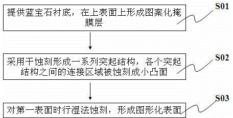
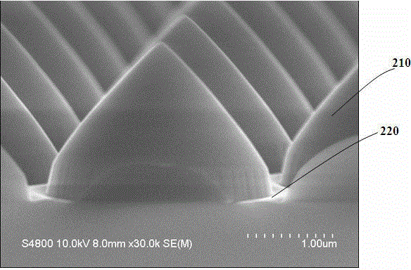
[0031] figure 1 Disclosed is a method for fabricating a patterned sapphire substrate, comprising steps S01 to S03, including forming a photomask layer, etching the substrate surface by dry etching, and forming a patterned surface without c-plane by wet etching the substrate surface .
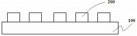
[0032] Step S01: Provide a sapphire substrate having opposite first and second surfaces, and form a patterned mask layer 200 on the first surface, such as figure 2 shown. The details are as follows: First, a layer of photoresist is coated on a flat sapphire substrate, and the thickness of the photoresist can be 0.5um to 3um; next, a pattern composed of a series of columnar photoresist is produced by using a yellow light process. This process can be Using a stepper exposure machine, contact exposure machine, projection exposure mach...
PUM
| Property | Measurement | Unit |
|---|---|---|
| thickness | aaaaa | aaaaa |
| thickness | aaaaa | aaaaa |
Abstract
Description
Claims
Application Information