Mems device and method of fabricating the same

A technology of micro-electromechanical systems and devices, which is applied to the components of TV systems, piezoelectric/electrostrictive/magnetostrictive devices, generators/motors, etc., can solve the problem of compatibility with IC processing and temperature tolerance Low, residual chemical gas overflow and other issues, to achieve the effect of strong mechanical and physical support

Active Publication Date: 2010-12-01
XIAN YISHEN OPTOELECTRONICS TECH CO LTD
View PDF6 Cites 20 Cited by
  • Summary
  • Abstract
  • Description
  • Claims
  • Application Information

AI Technical Summary

Problems solved by technology

However, the disadvantages of using photoresist as a sacrificial layer are: poor mechanical support for the top structural unit, low temperature tolerance for thin film processing, and residual chemical gas overflow, etc.
Other inorganic materials that can be used as sacrificial layers in the prior art can solve the above-mentioned problems caused by photoresist, but these materials are dissimilar materials or their dry etching removal process cannot be compatible with IC under the premise of satisfying the given selectivity requirements. Process Compatible

Method used


Image

  • Mems device and method of fabricating the same
  • Mems device and method of fabricating the same
  • Mems device and method of fabricating the same

Examples


Embodiment Construction

[0026] In order to make the purposes, technical solutions and advantages of the embodiments of the present invention clearer, the technical solutions in the embodiments of the present invention will be clearly and completely described below with reference to the accompanying drawings in the embodiments of the present invention. Obviously, the described embodiments These are some embodiments of the present invention, but not all embodiments. Based on the embodiments of the present invention, all other embodiments obtained by those of ordinary skill in the art without creative efforts shall fall within the protection scope of the present invention.

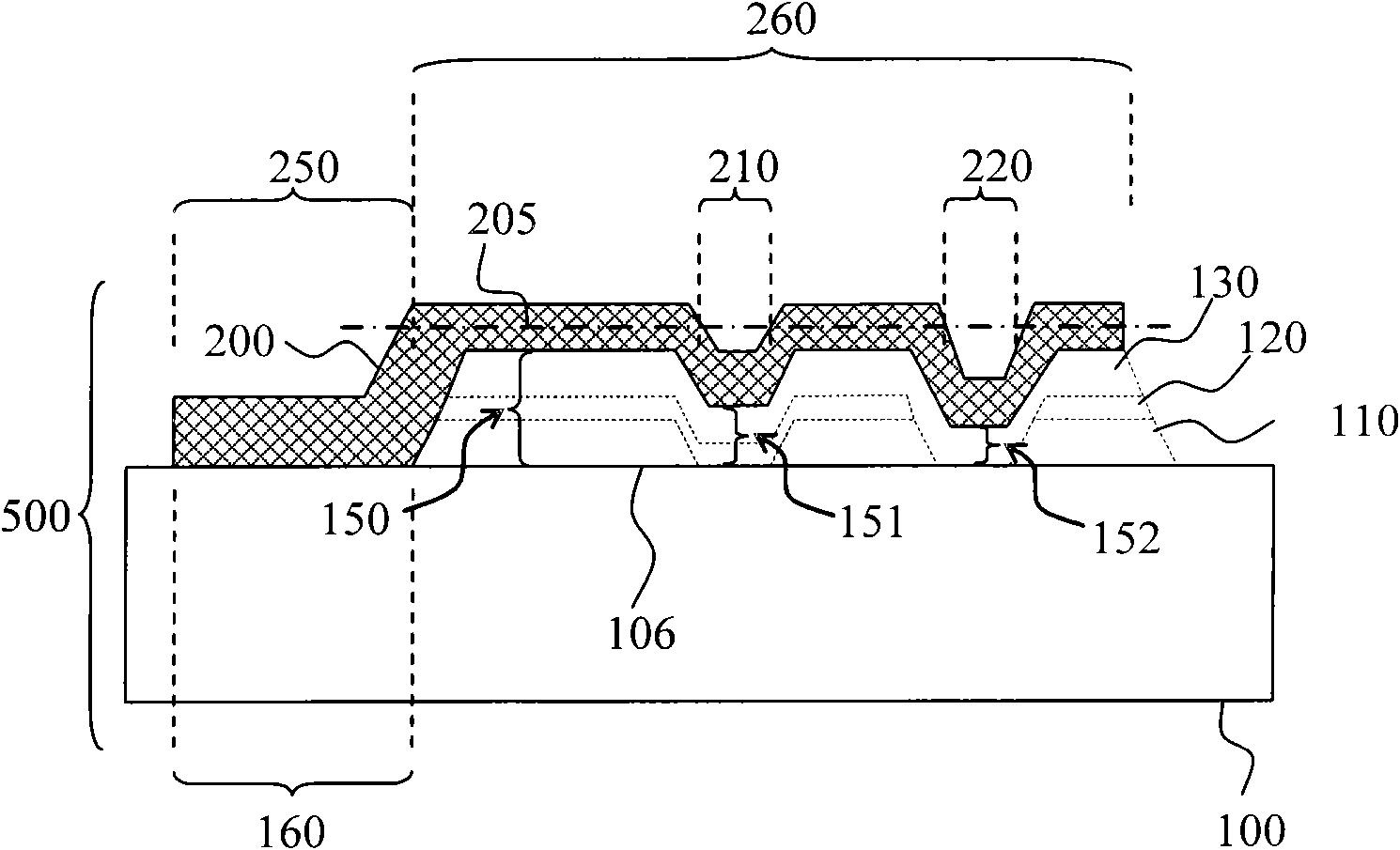
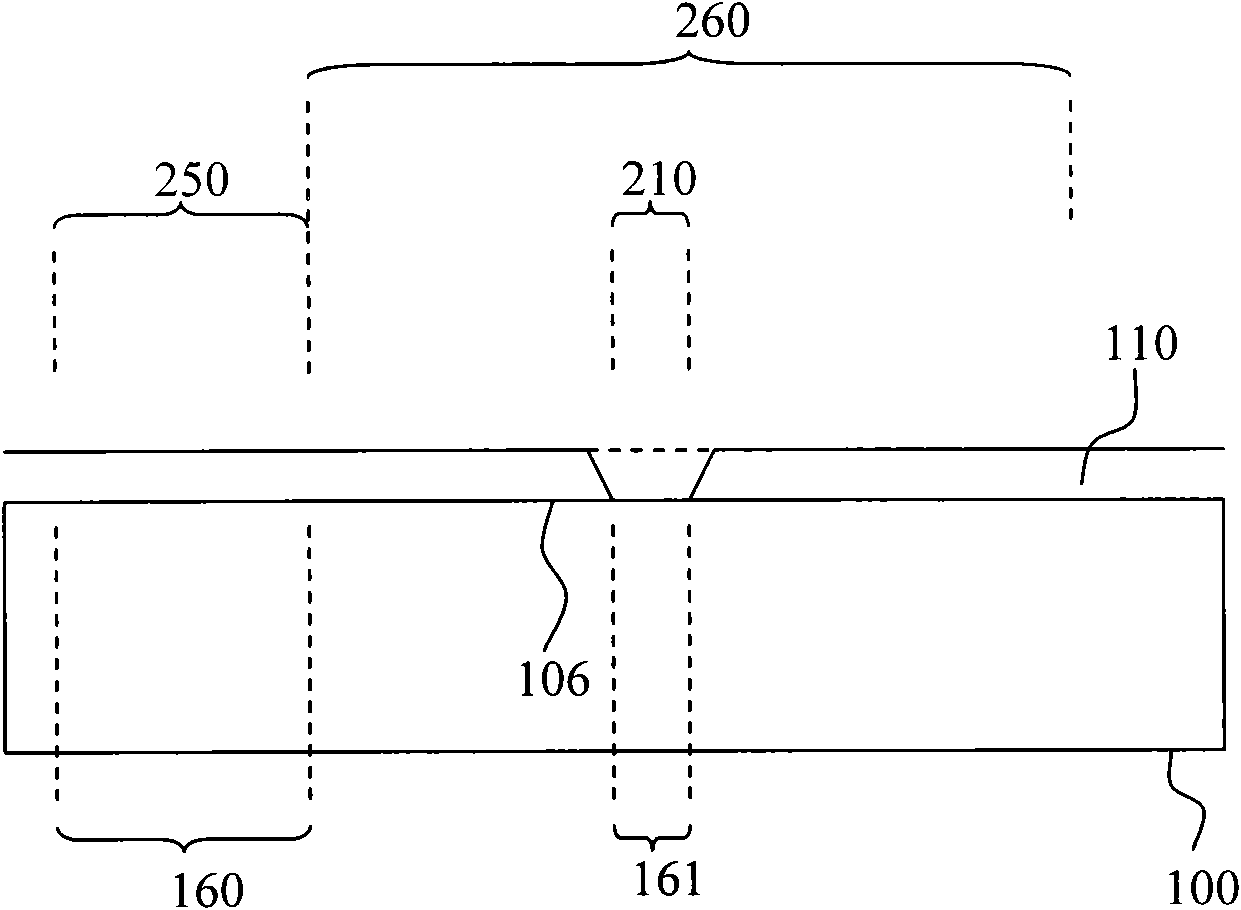
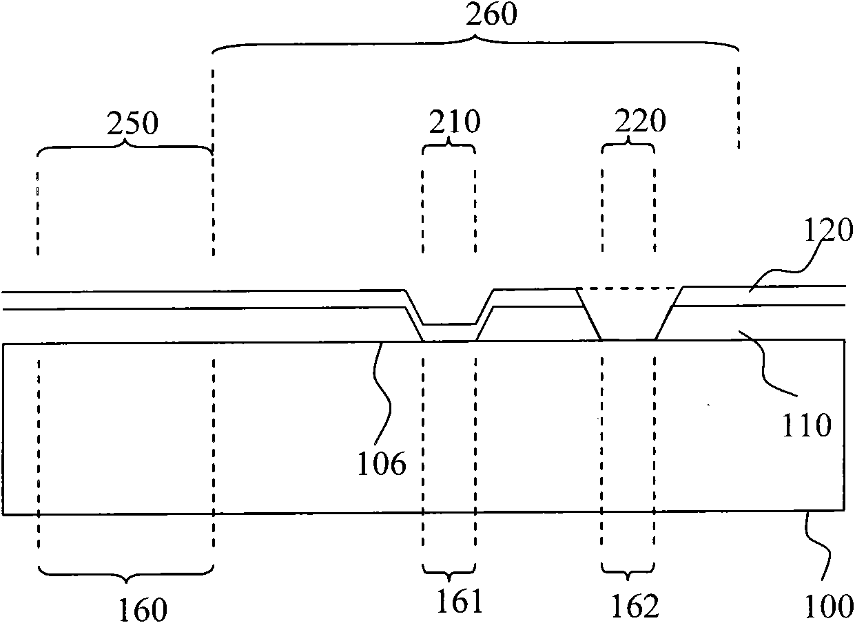
[0027] figure 1 It is a cross-sectional view of the MEMS device 500 according to an embodiment of the present invention, the MEMS device 500 includes a sacrificial layer using multiple layers of carbon films (ie, the first carbon film 110, the second carbon film 120 and the third carbon film 130) as the lower part The fabricated su...


PUM


Abstract

The present invention relates to a micro electrical-mechanical system (MEMS) device and a method of fabricating the same, wherein the device comprises a suspended thin film microstructure (200) arranged above a substrate (100), and is characterized in that the suspended thin film microstructure (200) includes an anchoring portion (250) adhered to the top surface (106) of the substrate (100); a suspended portion (260) arranged above the top surface (106) of the substrate (100) and having a base plane (205) configured in parallel to the substrate (100), and a base clearance is arranged between the base plane (205) and the top surface (106) of the substrate (100); the suspended portion (260) further includes a first recess portion (210) spaced at a first vertical clearance (151) with the top surface (106) of the substrate (100), the first vertical clearance (151) being configured differentially smaller than the base clearance (150). The invention is capable of providing strong mechanical and physical support force for sediment and lithographic patterns of a suspended construction unit.

Description

technical field [0001] The invention relates to a Micro-Electro-Mechanical System (Micro-Electro-Mechanical System, MEMS for short) device and a manufacturing method thereof. Background technique [0002] MEMS include integrated micro-devices, such as mechanical, optical and thermal sensing components, formed on a substrate, which is a single or composite layer of solid-state material. MEMS can be fabricated using existing wafer batch processing techniques to form the aforementioned microscopic devices, ranging in size from nanometers to millimeters, on solid-state substrates such as silicon wafers. These MEMS devices are used for sensing control at the microscale and perform various mechanical, optical, or chemical functions, either as a stand-alone single unit or in arrays that synergize within the microscale to produce an overall effect. Such MEMS devices can be applied but not limited to: accelerometers, gyroscopes, pressure sensors, chemical and flow sensors, micro-opt...

Claims


Application Information

Patent Timeline
Patent Type & Authority Applications(China)
IPC IPC(8): B81B7/02B81C1/00
CPCB81B2203/0307B81B2203/0118B81C1/0015B81C2203/0735B81C1/00246
Inventor 河·H·黄
Owner XIAN YISHEN OPTOELECTRONICS TECH CO LTD
Why Eureka
Try Eureka