Probe test circuit and design method thereof

A technology of test circuit and design method, which is applied in the direction of electronic circuit test, measuring circuit, measuring device, etc., can solve the problems of long development cycle, difficult maintenance and management, and high production cost of test probe card, so as to shorten the development cycle and reduce the The effect of fees

Active Publication Date: 2010-12-08
SINO IC TECH
View PDF5 Cites 4 Cited by
  • Summary
  • Abstract
  • Description
  • Claims
  • Application Information

AI Technical Summary

Problems solved by technology

[0007] In order to overcome the problems of high production cost, long development cycle and difficult maintenance and management of test probe car

Method used


Image

  • Probe test circuit and design method thereof
  • Probe test circuit and design method thereof
  • Probe test circuit and design method thereof

Examples


Embodiment Construction

[0019] The present invention will be further described below in conjunction with the accompanying drawings.

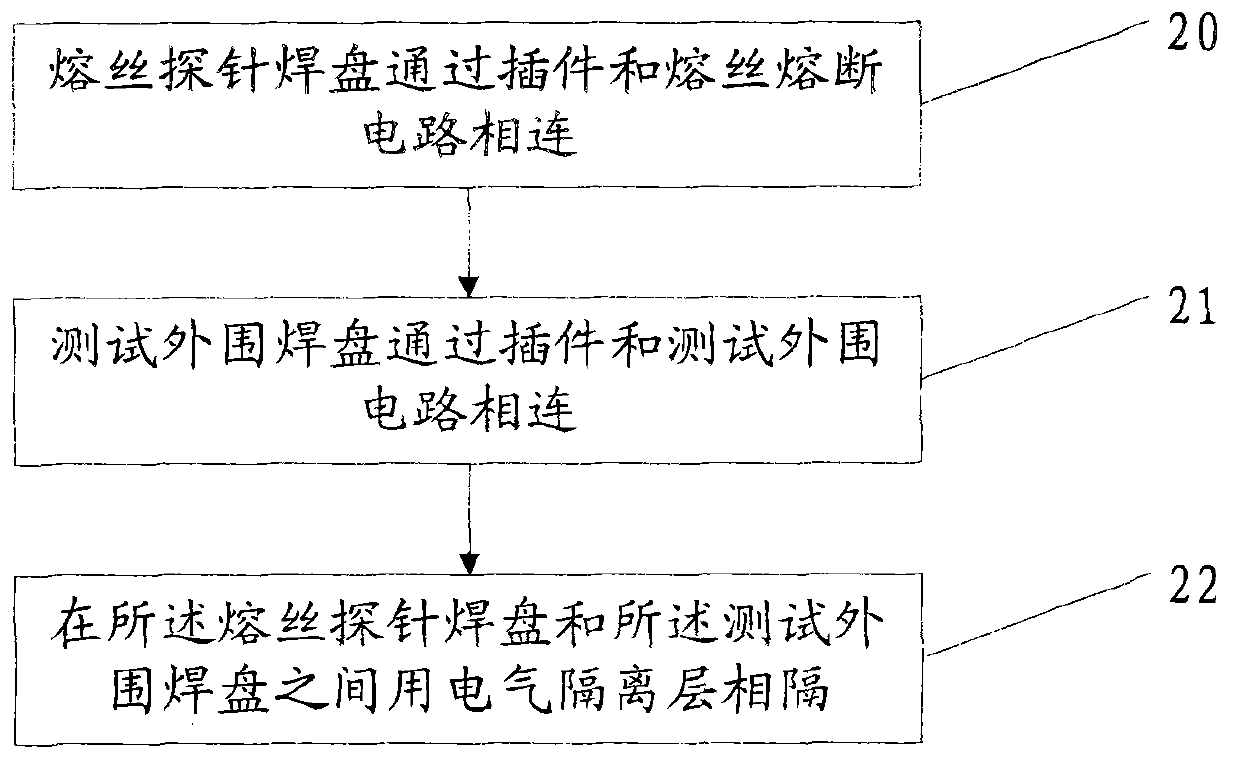
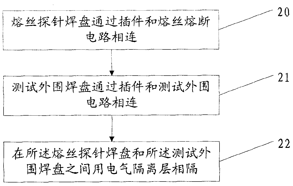
[0020] First, please refer to figure 1 , figure 1 It is a schematic flow chart of a probe test circuit and its design method in the present invention. As can be seen from the figure, the probe test circuit design method of the present invention includes the following steps:

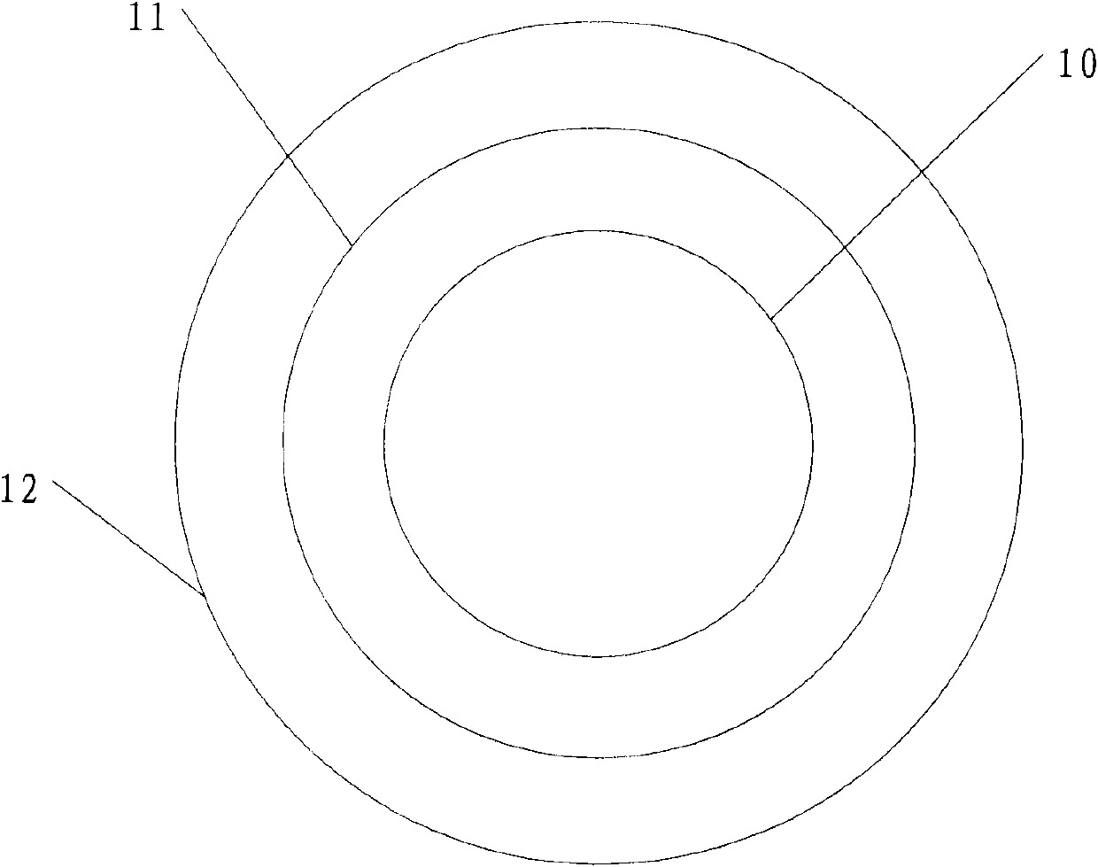
[0021] Step 20: The fuse probe pad is connected to the fuse blowing circuit through a plug-in. The plug-in is a European socket, and the fuse probe pad is ring-shaped. When assembling the test probe, it is only necessary to target For different types of chips, solder the fuse probes of related chips in the fuse probe pads;

[0022] Step 21: The test peripheral pad is connected to the test peripheral circuit through a plug-in, the test peripheral pad is ring-shaped, the plug-in is a European socket, the fuse probe pad is located in the test peripheral pad, and the fuse probe pad is located in the...


PUM


Abstract

The invention provides a probe test circuit and a design method thereof. The method comprises the following steps of: connecting a fuse wire probe pad and a fuse wire fusing circuit through a plug-in unit; connecting a peripheral test pad and a peripheral test circuit through a plug-in unit, wherein the fuse wire probe pad is positioned in the peripheral test pad; and separating the fuse wire probe pad and the peripheral test pad with an electric isolating layer. The probe test circuit and the design method thereof provided by the invention are easy for testing hardware and programs of development engineers, and production and maintenance of online product engineers, shorten the development period to the greatest degree and reduce the cost.

Description

technical field [0001] The invention relates to the field of integrated circuit chip testing, in particular to a probe testing circuit and a design method thereof. Background technique [0002] Power regulator chips are currently widely used in various consumer electronics devices, and have the advantages of stable output, small size, and high cost performance. In specific system applications, the power supply voltage regulator chip can output standard voltage values ​​such as 1.8v, 2.5v, 3.3v or customized voltage values, and the general error does not exceed 5%. In order to achieve the above specific voltage stability and small error, it is necessary to adjust the voltage of this type of chip in the chip wafer level test. The adjustment method and means are to change the output voltage by blowing the fuse combination inside the chip. value. In the actual wafer-level test mass production, various types of probe card boards for different types of chip models are required. ...

Claims


Application Information

Patent Timeline
IPC IPC(8): G01R1/02G01R1/067G01R31/28
Inventor 徐惠祁建华施瑾刘远华张志勇叶守银牛勇赵达君
Owner SINO IC TECH
Why Eureka
Try Eureka