Single-event effect detection device and method

A single-event effect and detection device technology, applied in the field of space radiation effect detection, can solve the problems of high quality, volume, power consumption of detectors, thick effective thickness of semiconductor detectors, and inaccurate measurement of heavy ions, etc. effect of low power consumption and wide measurement range

Inactive Publication Date: 2010-12-08
CENT FOR SPACE SCI & APPLIED RES
View PDF0 Cites 26 Cited by
  • Summary
  • Abstract
  • Description
  • Claims
  • Application Information

AI Technical Summary

Problems solved by technology

However, due to the limitation of the reliability of space applications, the effective thickness of the semiconductor detectors that can be used is relatively thick, usually about 400 μm, which is the same as the thickness of the current microelectronic devices that are sensitive to single event effects, which is on the order of microns or ten microns. far from
Due to the large effective detection thickness, the LET value of this technology for inducing the single event effect of modern technology devices is several MeV.cm 2 The measurement of heavy ions per mg is inaccurate or even impossible, which is especially unfavorable for measuring the complex particle environment that can induce single event effects in the accessories of key components on the star
For detecting the proton single-event effect of VHLET events formed by secondary heavy ions generated by nuclear reactions, it is effective to detect the distribution of VHLET spectra measured by extremely thick detectors and the actual VHLET spectra occurring in extremely small microelectronic devices Therefore, it is difficult to correctly infer the degree of proton single event effect actually occurring in microelectronic devices by using this detection result
[0010] On the other hand, this semiconductor detector-based detection technology uses the traditional particle energy measurement technology, which requires a relatively large mass, volume, and power consumption of the detector.

Method used


Image

  • Single-event effect detection device and method
  • Single-event effect detection device and method
  • Single-event effect detection device and method

Examples


Embodiment Construction

[0036] The present invention will be further described in detail below in conjunction with the accompanying drawings and specific embodiments.

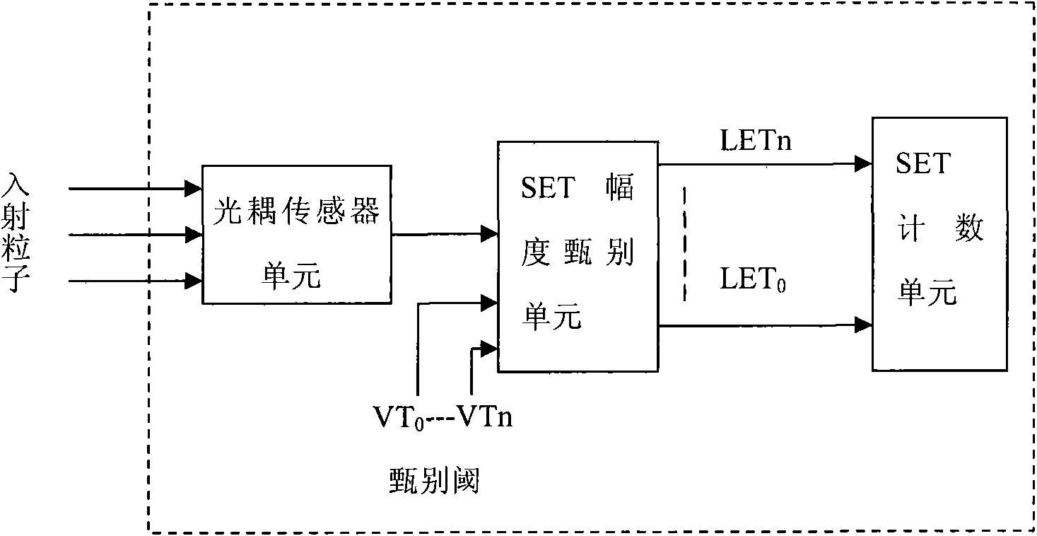
[0037]The single event effect that occurs in optoelectronic devices and analog devices is manifested by the fact that after the sensitive parts of these devices are hit by a single particle, an abnormal output pulse is generated at the output of the device, which is called a single event transient pulse (Single Event Transient, SET) effect. Utilizing the single event transient pulse effect, the present invention proposes a single event effect detection device and method based on a single event transient pulse (SET) of a photoelectric coupling device (optocoupler for short). In this embodiment, by measuring the SET analog signal generated by a single high-energy particle bombarding the optocoupler in the radiation environment, according to the correlation between the amplitude of the SET and the LET value of the incident particle, the ...


PUM


Abstract

The invention provides a single-event effect detection device, which comprises a light-coupler sensor working unit, an SET amplitude discriminator unit and an SET counting unit, wherein the light-coupler sensor working unit is used for acquiring an SET signal from a radiation environment to be detected; the SET amplitude discriminator unit is used for comparing the SET signal amplitude obtained by the light-coupler sensor working unit with a threshold voltage to discriminate the amplitude ranges of different SET signals; and the SET counting unit is used for counting the number of the SET signals in each amplitude range. The device may also comprise a data mapping unit. The device and the method can realize the measurement of the values of several or tens of MeV.cm<2> / mg LETs and the measurement of the radiation environment of lower magnitudes and quantitatively measure the LET value for characterizing the single event effect of a specific micro electronic element, has a wider LET value quantitative measurement range. In addition, the used sensor has a small volume and small mass; the circuit structure is simple; and the lightening, miniaturization and low power consumption of the detection device can be realized easily.

Description

technical field [0001] The invention relates to the field of space radiation effect detection, in particular, the invention relates to a single event effect detection device and method. Background technique [0002] The space environment is an important factor that endangers the safety and reliability of spacecraft. The space radiation effect is a prominent environmental effect that induces spacecraft anomalies or failures. Radiation environments such as high-energy charged particles in space, magnetospheric substorm injection, and auroral subsidence plasma are likely to induce a series of radiation effects such as total dose effect, single event effect, surface and deep charging effect, among which single event effect is the one that induces spacecraft anomalies Or one of the most malfunctioning radiation effects. On the basis of in-depth research on the single event effect and protection technology of digital integrated circuits, the international aerospace community has...

Claims


Application Information

Patent Timeline
Patent Type & Authority Applications(China)
IPC IPC(8): G01R31/00G01R31/316
Inventor 韩建伟马英起封国强安广鹏张振龙
Owner CENT FOR SPACE SCI & APPLIED RES
Why Eureka
Try Eureka