Homogeneous beam spot method for electron beam surface treatment

A surface treatment and electron beam technology, applied in the field of uniform beam spot and electron beam surface treatment, can solve the problems of small thermal action area and uneven heating of the material surface, and achieve good economical effects

Active Publication Date: 2012-09-05
NO 510 INST THE FIFTH RES INST OFCHINA AEROSPAE SCI & TECH
View PDF1 Cites 0 Cited by
  • Summary
  • Abstract
  • Description
  • Claims
  • Application Information

AI Technical Summary

Problems solved by technology

[0005] The purpose of the present invention is to solve the problems of uneven heating of the material surface and small heat action area caused by the use of circular beam spots when the existing electron beam is used for surface treatment, and to propose a uniform surface treatment method for electron beam surface treatment. beam spot method

Method used


Image

  • Homogeneous beam spot method for electron beam surface treatment
  • Homogeneous beam spot method for electron beam surface treatment
  • Homogeneous beam spot method for electron beam surface treatment

Examples


example 1

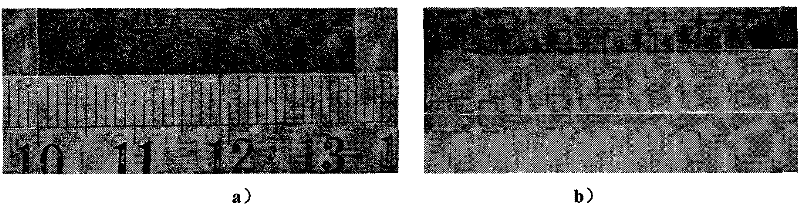
[0028] Example 1 TC4 titanium plate test

[0029] Step 1: Large-area uniform beam spot waveform design

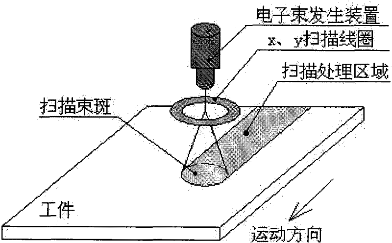
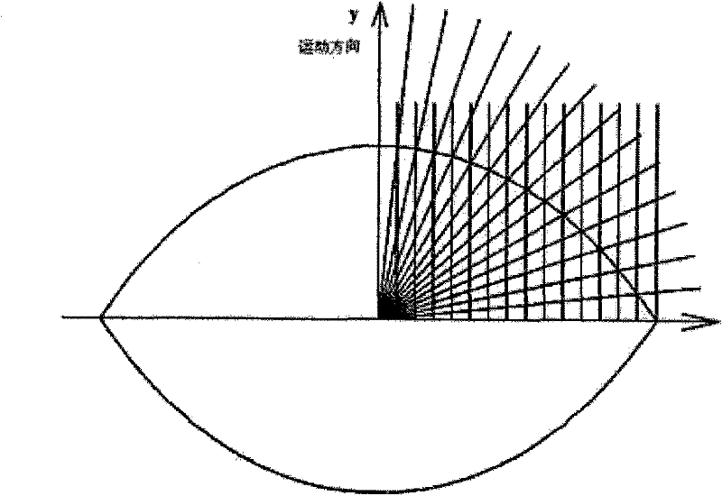
[0030] The scanning system of the electron beam is composed of two mutually perpendicular electromagnetic coils at the bottom of the electron gun. Under the action of the two-dimensional magnetic field, the electron beam can realize non-contact deflection and produce any two-dimensional plane graphics; With different magnetic field signals, the electron beam can produce various patterns of electron beam trajectories under the action of different magnetic fields, such as figure 1 shown;

[0031] The electrons move at a very high speed. Within a certain period of time, the heating sequence caused by the two-dimensional plane graphics generated by the electron beam scanning during the heating process can be ignored; as the workpiece moves, the component of the electron beam energy perpendicular to the direction of motion is guaranteed. Equal, so that the heating of the treat...

example 2

[0045] Example 2 Silicide coating cladding treatment test

[0046] Step 1: Large-area uniform beam spot waveform design

[0047] The scanning system of the electron beam is composed of two mutually perpendicular electromagnetic coils at the bottom of the electron gun. Under the action of the two-dimensional magnetic field, the electron beam can realize non-contact deflection and produce any two-dimensional plane graphics; With different magnetic field signals, the electron beam can produce various patterns of electron beam trajectories under the action of different magnetic fields, such as figure 1 shown;

[0048] Electrons move at a very high speed. Within a certain period of time, the heating sequence caused by the two-dimensional plane graphics generated by electron beam scanning during the heating process can be ignored; The components are equal, thus ensuring the uniformity and consistency of heating in the treated area;

[0049] The specific method is: divide the x-ax...


PUM


Abstract

The invention relates to an electron beam surface treatment method, in particular to homogeneous beam spot technology in electron beam surface treatment technology, belonging to the technical field of surface treatment. The homogeneous beam spot technology for electron beam surface treatment mainly comprises the steps of beam spot waveform design, programming and process test and optimization, etc. The technology is characterized by designing the homogeneous beam spot waveform in conformity with the requirement of surface treatment according to the electron beam scanning principle and the energy distribution law in the movement process, carrying out curve fitting on the beam spot waveform by the least square method in a Cartesian coordinate system, programming the fitting result and storing the programmed fitting result into a computer control system, carrying out test and optimization by controlling the process parameters of electron beam surface treatment and finally obtaining large-area homogeneous beam spot technology. The method is easier to realize, has better economical efficiency, overcomes the defect that the energy of other electro beam spots are not distributed homogeneously, dispenses with extra control equipment and can be directly realized on the general electron beam equipment.

Description

technical field [0001] The invention relates to an electron beam surface treatment method, in particular to a uniform beam spot method in the electron beam surface treatment technology, and belongs to the technical field of surface treatment. Background technique [0002] In recent years, the method of using high-energy beams (electron beams, ion beams, laser beams) to modify the surface of metal materials has been developed rapidly. Because the utilization rate of electron beam energy (up to 90%) does not depend on the characteristics of the surface of the material, it is not disturbed by the process atmosphere, and the power is large, the use of electron beams for display processing technology is becoming one of the current attractive technologies. [0003] In order to meet the needs of different workpieces and different cladding requirements, the electron beam cladding equipment must have a variety of beam spot scanning functions to realize the application of beam spot de...

Claims


Application Information

Patent Timeline
Patent Type & Authority Patents(China)
IPC IPC(8): H01J37/304H01J37/32
Inventor 张永和何俊于斌张涛王世伟
Owner NO 510 INST THE FIFTH RES INST OFCHINA AEROSPAE SCI & TECH
Why Eureka
Try Eureka