Etching device and method

An etching device and etching technology are applied in the direction of electrical components, semiconductor/solid-state device manufacturing, circuits, etc., which can solve the problems of uneven etching and inaccurate etching rate control, etc., and achieve the effect of precise control

Inactive Publication Date: 2010-12-22
SEMICON MFG INT (SHANGHAI) CORP
View PDF1 Cites 0 Cited by
  • Summary
  • Abstract
  • Description
  • Claims
  • Application Information

AI Technical Summary

Problems solved by technology

[0007] The present invention solves the problem that the etching rate control of d...

Method used


Image

  • Etching device and method
  • Etching device and method
  • Etching device and method

Examples


Embodiment approach

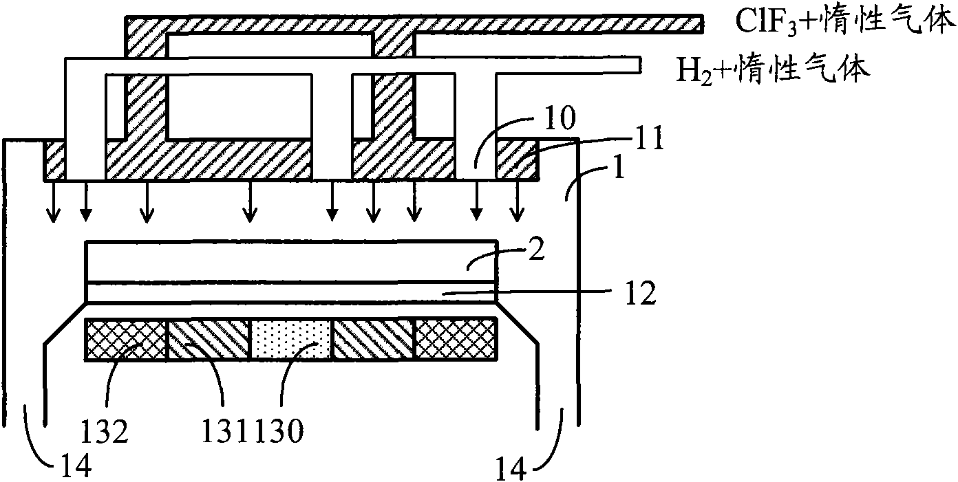
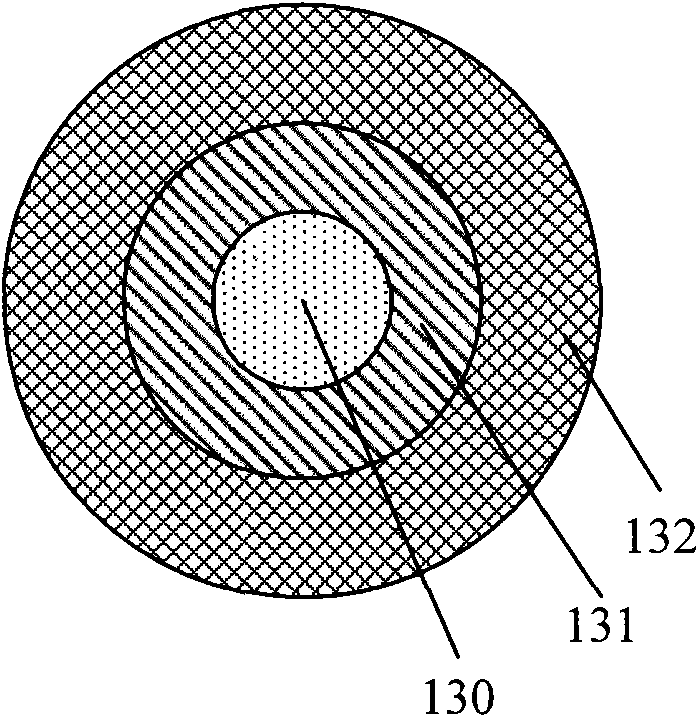
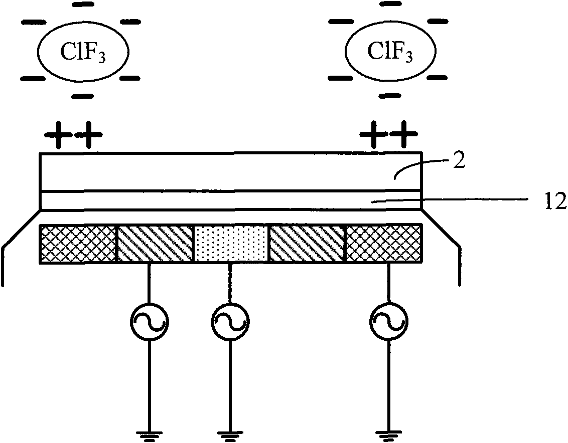
[0017] Based on this, the present invention provides an etching device. According to one embodiment, the etching device includes a cavity with a plurality of air inlets, and a wafer tray is provided in the cavity for carrying a wafer. The cavity also includes a plurality of etching control units located under the wafer tray, and the etching control units are used to control the voltage of the corresponding wafer to be etched, and the polarity of the voltage is the same as that passed into the cavity through the air inlet. The polarity of the charged etching gas is opposite.

[0018] In the embodiment of the above etching device, the etching control unit applies a voltage opposite in polarity to the charged etching gas at the corresponding position of the wafer to be etched, and forms a corresponding electric field at the position to be etched. Due to the principle of attraction of opposites, the etching gas will be adsorbed at the position of the wafer to be etched, thereby pe...


PUM


Abstract

The invention discloses an etching device and an etching method. The etching device comprises a chamber with a plurality of gas inlets, wherein a wafer tray is arranged in the chamber for carrying a wafer; the chamber also comprises a plurality of etching control units which are positioned below the wafer tray; the etching control units are used for controlling voltage of corresponding to-be-etched positions of the wafer; and the polarity of the voltage is reverse to that of a charged etching gas introduced into the chamber through the gas inlets. The etching device is also provided with a plurality of gas outlets which are connected with a vacuum-pumping system through valves for controlling pressure during etching. The gas inlets are also connected with an inert gas source for providing an inert gas through conduction valves. Through the etching device and the etching method, the etching rate can be controlled well and the etching uniformity is high.

Description

technical field [0001] The invention relates to the field of semiconductor manufacturing, in particular to an etching device and method. Background technique [0002] With the development of semiconductor manufacturing technology, the integration level of semiconductor devices is getting higher and higher. Existing semiconductor devices all have a multilayer structure. In the process of manufacturing semiconductor devices, in order not to affect subsequent processes such as material growth, the surface of each layer of material is usually polished after forming a layer of material (for example, after a layer of material is formed by chemical vapor deposition). , so that the surface flatness of this layer of material meets the requirements of the process. [0003] In the polishing step, the most commonly used method is chemical mechanical polishing. The advantage of chemical mechanical polishing is that it can grind the surface of the material faster. However, due to the ...

Claims


Application Information

Patent Timeline
IPC IPC(8): H01L21/00H01L21/3065H01L21/311H01L21/3213C23F4/00
Inventor 三重野文健
Owner SEMICON MFG INT (SHANGHAI) CORP
Why Eureka
Try Eureka