System and method for inspecting a wafer

A wafer and defect detection technology, used in measurement devices, semiconductor/solid-state device testing/measurement, image data processing, etc.

Active Publication Date: 2010-12-22
SEMICON TECH & INSTR
View PDF4 Cites 23 Cited by
  • Summary
  • Abstract
  • Description
  • Claims
  • Application Information

AI Technical Summary

Problems solved by technology

However, due to the current lack of professional technical knowledge and operational skills, despite the flexibility in design and construction, existing semiconductor wafer inspection systems cannot simultaneously perform bright-field and dark-field imaging for inspection while the wafer is moving.

Method used


Image

  • System and method for inspecting a wafer
  • System and method for inspecting a wafer
  • System and method for inspecting a wafer

Examples


Embodiment Construction

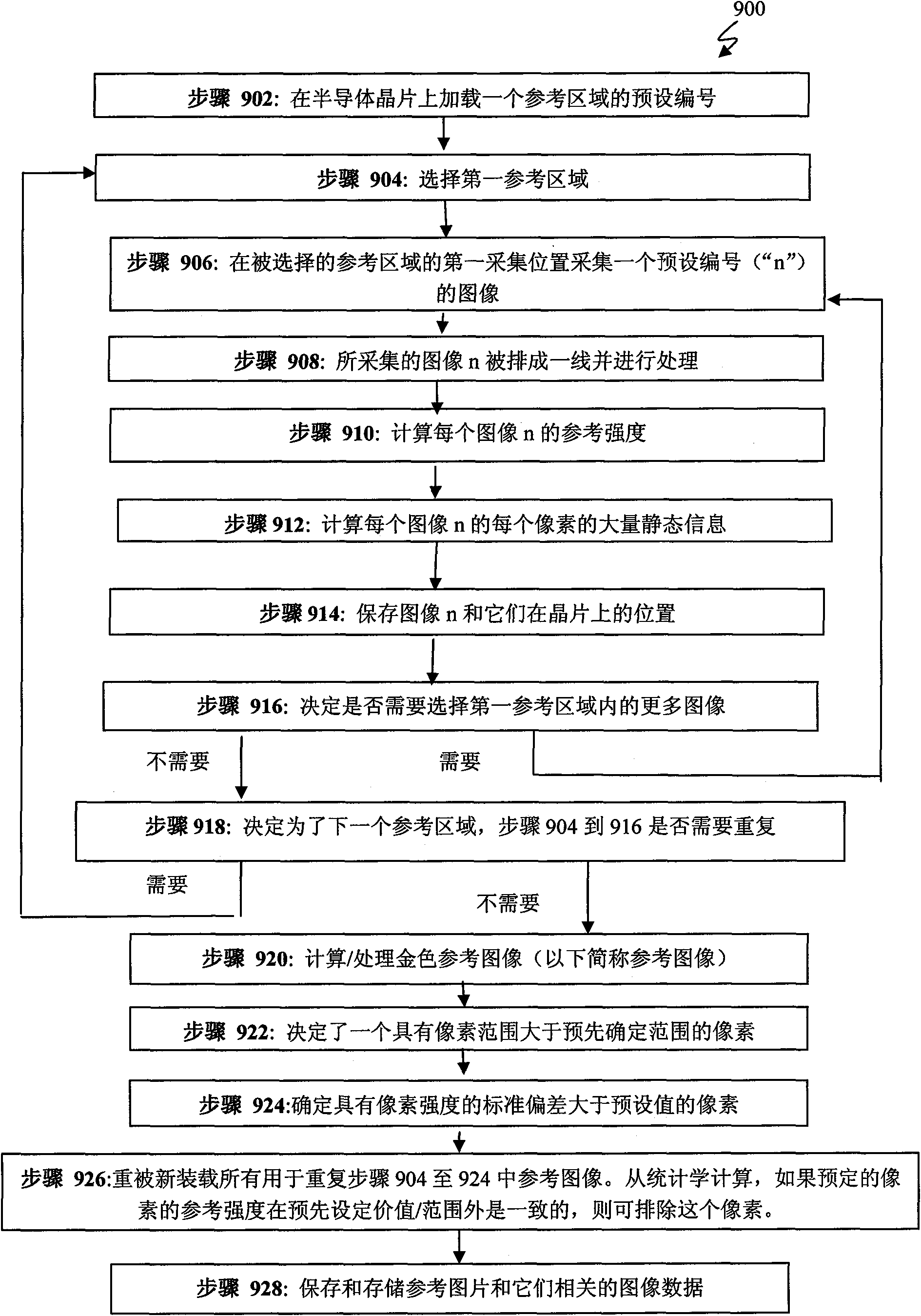
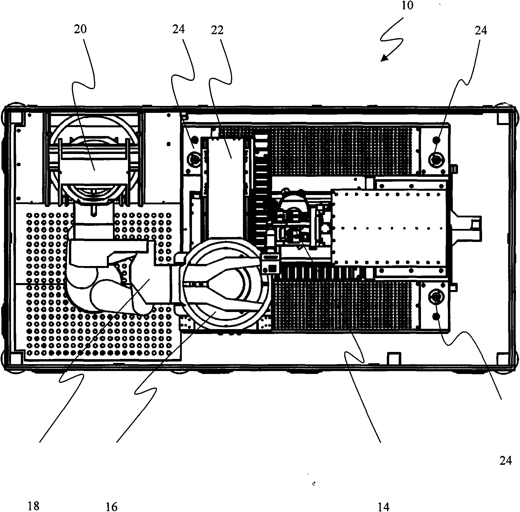
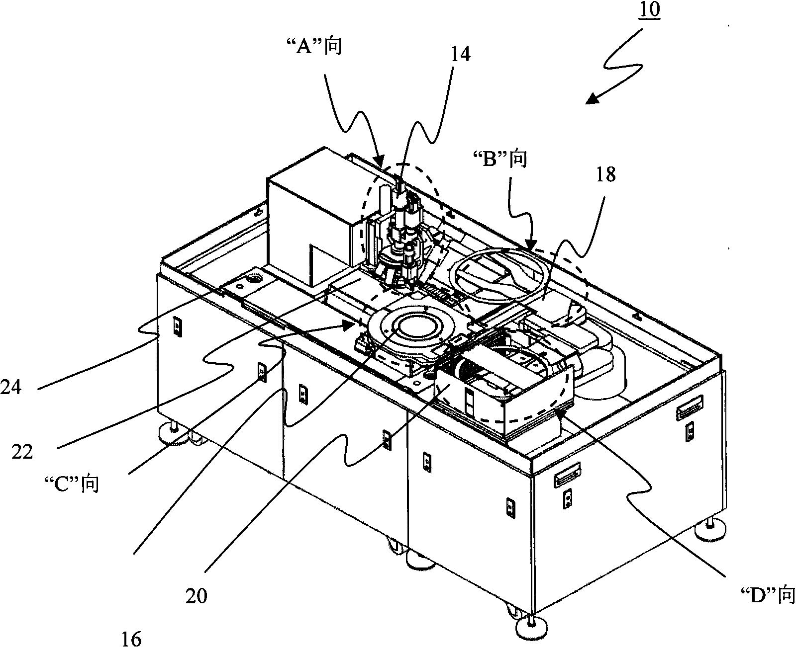
[0063] The inspection of semiconductor components, eg semiconductor wafers and chips, is an increasingly important step in the processing and manufacturing of semiconductors. Due to the increasing complexity of circuits on semiconductor wafers and the improvement of quality standards for semiconductor wafers, there is an increasing need for improved inspection systems and inspection methods for semiconductor wafers.

[0064] Although current semiconductor wafer inspection systems and inspection methods can provide configuration and design flexibility, they cannot simultaneously generate bright-field and dark-field images for dynamic inspection of semiconductor wafers. In addition, flexibility in the semiconductor wafer inspection system is required And the components of the relevant structure of the adjustable space, such as illuminator, camera or image acquisition device, objective lens, filter and its mirror. Due to the increasing complexity of semiconductor wafer electronic...


PUM

PropertyMeasurementUnit
wavelengthaaaaaaaaaa

Abstract

A method and a system for inspecting a wafer. The system comprises an optical inspection head, a wafer table, a wafer stack, a XY table and vibration isolators. The optical inspection head comprises a number of illuminators, image capture devices, objective lens and other optical components. The system and method enables capture of brightfield images, darkfield images, 3D profile images and review images. Captured images are converted into image signals and transmitted to a programmable controller for processing. Inspection is performed while the wafer is in motion. Captured images are compared with reference images for detecting defects on the wafer. An exemplary reference creation process for creating reference images and an exemplary image inspection process is also provided by the present invention. The reference image creation process is an automated process.

Description

technical field [0001] The invention relates to a process of wafer inspection. In particular, it relates to automated systems and methods for inspecting semiconductor components. Background technique [0002] The ability to assure the quality of the production of semiconductor components, such as semiconductor wafers and chips, is of increasing importance in semiconductor manufacturing. The manufacturing process of semiconductor wafers has been continuously improved to incorporate an increasing number of feature sizes into semiconductor wafers with small surface areas. As a result, photolithographic processes are becoming more sophisticated for the production of semiconductor wafers, allowing an increasing number of feature sizes to be incorporated into semiconductor wafers with smaller surface areas (eg, resulting in higher performance semiconductor wafers). Therefore, the size of possible errors on a semiconductor wafer is typically in the micron to sub-micron range. ...

Claims


Application Information

Patent Timeline
Patent Type & Authority Applications(China)
IPC IPC(8): H01L21/66G01N21/892
CPCH01L22/12G06T2207/20212G01N21/9501G06T2207/10152G01N21/8806G06T2207/30148G06T7/001G01N2021/8825
Inventor 阿杰亚拉里·阿曼努拉葛汉成
Owner SEMICON TECH & INSTR
Why Eureka
Try Eureka