Camera system with multiple pixel arrays on chip

A camera and pixel technology, applied in signal generators with multiple pickup devices, components of TV systems, image communication, etc. Cost, Small Design, Low Power Effect

Active Publication Date: 2010-12-22
CAPSO VISION INC
View PDF3 Cites 71 Cited by
  • Summary
  • Abstract
  • Description
  • Claims
  • Application Information

AI Technical Summary

Problems solved by technology

As a result, such systems have large power consumption caused by repeated signal chains on the chip
Such systems are also more complex and bulky due to the difficulty of aligning multiple chips, and can be more expensive to manufacture

Method used


Image

  • Camera system with multiple pixel arrays on chip
  • Camera system with multiple pixel arrays on chip
  • Camera system with multiple pixel arrays on chip

Examples


Embodiment Construction

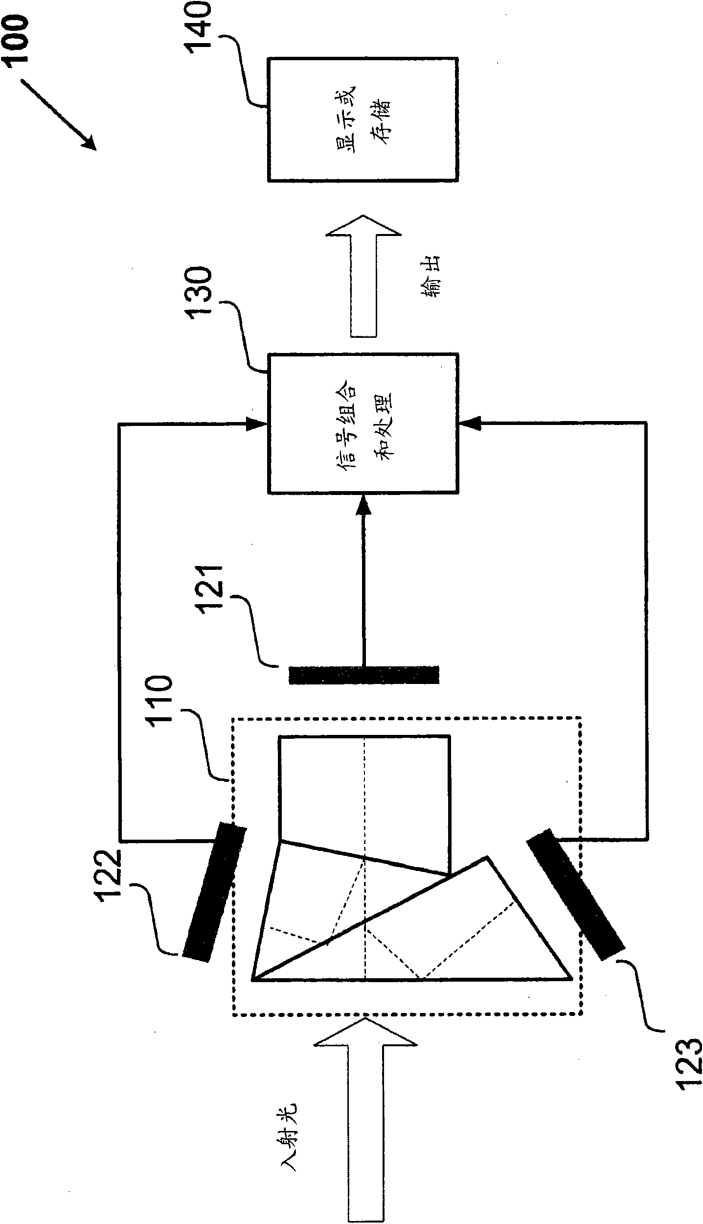
[0021] The present invention provides a camera system having a plurality of pixel arrays on a semiconductor substrate ("on-chip"). figure 1 A conventional camera system 100 with multiple image sensor chips is shown. Such as figure 1 As shown in , the camera system 100 includes an optical system 110 , a plurality of image sensor IC chips 121 , 122 and 123 , a signal processing circuit 130 , and a display or storage element 140 . Optical system 110, typically including a lens and a beam splitter, forms a plurality of images from incident light. The plurality of light sensing chips 121, 122, and 123 are aligned with the positions of the plurality of images within the depth of focus, and convert the sensed light into electrical signals in the analog or digital domain. The signal processing circuit 130 then combines the output signals from the plurality of image sensors 121, 122 and 123 for further processing. The output signal from the signal processing circuit 130 is sent to a...


PUM


Abstract

A camera system uses one or more image sensor IC chips each having multiple pixel arrays on the same semiconductor substrate (i.e., ''multiple pixel arrays on a chip''). In one embodiment, such a camera system includes: (a) optical components that create multiple images in dose physical proximity of each other (e.g., within a few millimeters or 10 centimeters); and (b) a single sensor substrate (''chip'') containing multiple 2 -dimensional pixel arrays that are aligned to capture these multiple images, so as to convert the multiple images into electrical signal. The pixel arrays can be manufactured using a CCD or a CMOS compatible process. Such a chip is typically two centimeters or less on a side. Optional electronic components for further signal processing of the captured images may be formed either on the sensor chip (i.e., in a ''system-on-a-chip'' implementation), or in a separate back-end application specific integrated circuit (ASIC).

Description

[0001] Cross References to Related Applications [0002] This application is related to, and claims priority to, the following applications: (a) U.S. Provisional Patent Application Serial No. 60 / 2007, entitled "Camera System Having Multiple Pixel Arrays on a Chip," filed November 27, 2007. 990,601; and (b) U.S. Nonprovisional Patent Application Serial No. 12 / 323,219, filed November 25, 2008, entitled "Camera System Having Multiple Pixel Arrays on a Chip," both of which are incorporated by reference incorporated here. For US designations, this application is a continuation of the aforementioned US patent application no. 12 / 323219. technical field [0003] The present invention relates generally to optical camera systems. More specifically, the present invention relates to optical camera systems using integrated circuits (ICs) that integrate two or more separate arrays of imaging pixels on a single IC chip. Background technique [0004] An optical camera system typically in...

Claims


Application Information

Patent Timeline
Patent Type & Authority Applications(China)
IPC IPC(8): H04N7/00G02B13/06H04N5/369H04N7/24H04N9/09
CPCH04N5/3745H04N5/23238H04N5/378A61B1/041G02B13/06H04N5/3415H04N23/698H04N25/41H04N25/77H04N25/75
Inventor 骆稼夫王康怀戈登·威尔逊
Owner CAPSO VISION INC
Why Eureka
Try Eureka