CMOSFETs structure for controlling threshold voltage of device and manufacturing method thereof

一种阈值电压、制造方法的技术,应用在半导体/固态器件制造、半导体器件、电路等方向,达到控制阈值电压、增强界面偶极子的效果

Active Publication Date: 2010-12-29
INST OF MICROELECTRONICS CHINESE ACAD OF SCI
View PDF4 Cites 8 Cited by
  • Summary
  • Abstract
  • Description
  • Claims
  • Application Information

AI Technical Summary

Problems solved by technology

On the other hand, due to the Fermi level pinning effect, V fb Due to the existence of problems such as roll-off effect, the adjustment of the threshold voltage of NMOS devices and PMOS devices using the above methods can only be limited within a certain range.

Method used


Image

  • CMOSFETs structure for controlling threshold voltage of device and manufacturing method thereof
  • CMOSFETs structure for controlling threshold voltage of device and manufacturing method thereof
  • CMOSFETs structure for controlling threshold voltage of device and manufacturing method thereof

Examples


Embodiment Construction

[0040] In order to make the object, technical solution and advantages of the present invention clearer, the present invention will be described in further detail below in conjunction with specific embodiments and with reference to the accompanying drawings.

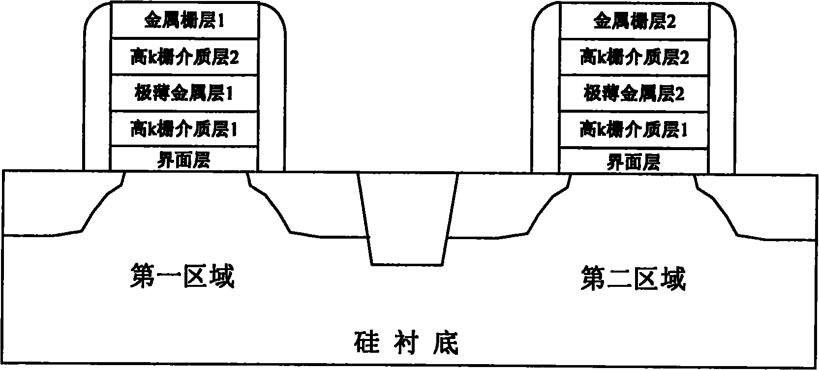
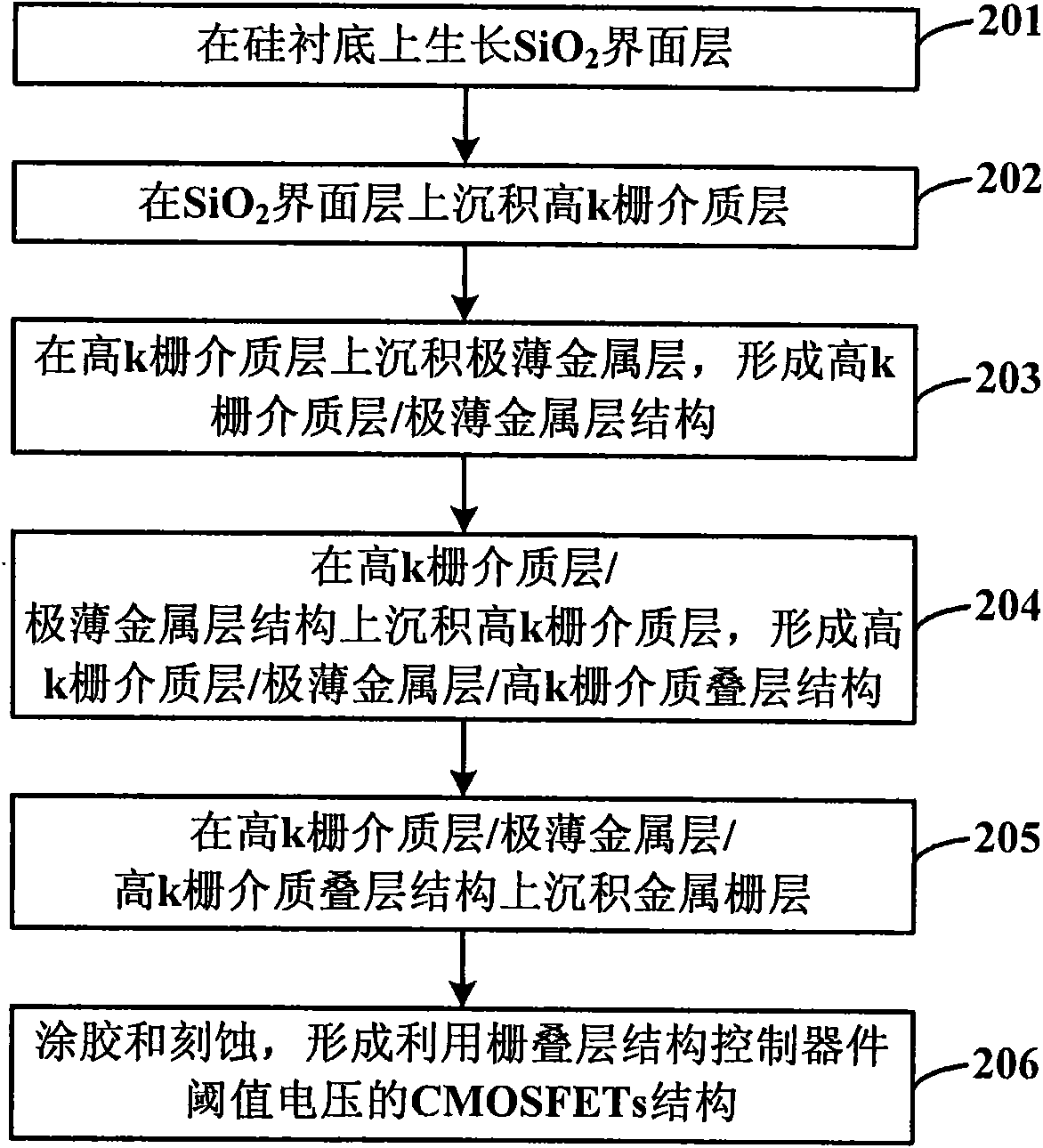
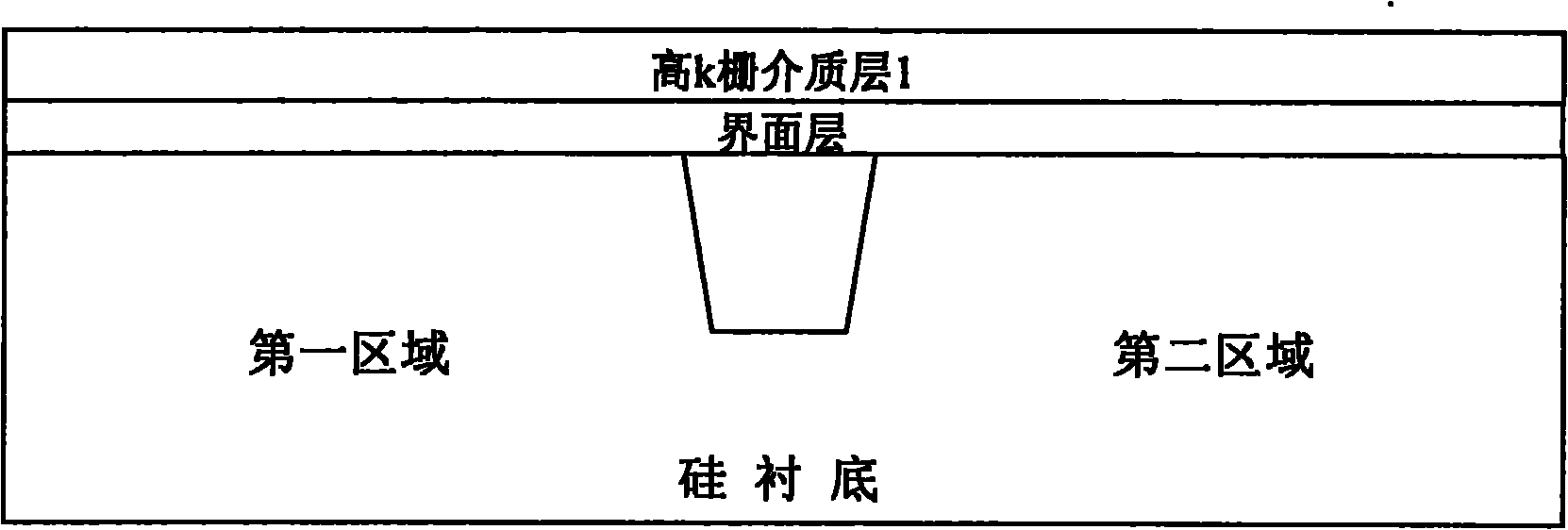
[0041] The CMOSFETs structure and its manufacturing method which utilize gate stack structure to control device threshold voltage provided by the present invention are to respectively deposit an extremely thin metal layer inside the high-k gate dielectric layer in the NMOS and PMOS device regions, and utilize the extremely thin metal layer The positive or negative charge formed inside the high-k gate dielectric layer adjusts the flat-band voltage of the device, thereby controlling the threshold voltage of the device. By adopting this process, not only the high-k gate dielectric and SiO2 in CMOS devices can be enhanced 2 The interface dipole between the interface layers can also control the type and quantity of fixed charg...


PUM


Abstract

The invention discloses a CMOSFETs structure for controlling the threshold voltage of a device by using a gate stack structure and a manufacturing method thereof. The structure comprises a silicon substrate, a SiO2 boundary layer growing on the silicon substrate, a high k gate dielectric layer deposited on the SiO2 boundary layer, an ultra thin metal layer deposited on the high k gate dielectric layer, a high k gate dielectric layer deposited on the ultra thin metal layer structure and a metal gate layer deposited on the high k gate dielectric stack structure. The manufacturing method comprises the following steps: respectively depositing the ultra thin metal layers in the high k gate dielectric layers in the regions of NMOS and PMOS devices, and regulating the flat band voltage of the devices by using positive or negative charges formed by the ultra thin metal layers in the high k gate dielectric layers, thereby controlling the threshold voltage of the devices. The invention not only can enhance the interface dipole between the high k gate dielectric layer and the SiO2 boundary layer in the CMOS device, but also can well control the type and the number of permanent charges in the high k gate dielectric layer, thereby effectively controlling the threshold voltage of the device.

Description

technical field [0001] The invention relates to the technical field of high-k gate dielectric and metal gate structure in nanotechnology CMOS technology, in particular to a CMOSFETs structure and a manufacturing method thereof which utilize a gate stack structure to control device threshold voltage. Background technique [0002] The application of key core technologies of 22nm and below process integrated circuits is an inevitable trend in the development of integrated circuits, and it is also one of the topics that major international semiconductor companies and research organizations are competing to research and develop. CMOS device gate engineering research centered on "high-k gate dielectric / metal gate" technology is the most representative key core process in 22nm and below technologies, and related material, process and structure research has been extensively carried out middle. [0003] For a CMOS device with a high-k gate dielectric / metal gate structure, its leakag...

Claims


Application Information

Patent Timeline
Patent Type & Authority Applications(China)
IPC IPC(8): H01L27/092H01L29/423H01L29/49H01L29/51H01L21/8238H01L21/28H01L21/283
CPCH01L27/092H01L29/7833H01L21/823857H01L29/513H01L29/6659H01L29/517
Inventor 王文武朱慧珑陈世杰陈大鹏
Owner INST OF MICROELECTRONICS CHINESE ACAD OF SCI
Why Eureka
Try Eureka