

GaN longitudinal reverse conducting junction field effect transistor
A junction field effect and reverse conduction technology, applied in semiconductor devices, electrical components, circuits, etc., can solve problems such as increasing parasitic capacitance and parasitic inductance, current collapse, excessive turn-on voltage, etc., and achieve off-state withstand voltage power consumption, The effect of adjustable threshold voltage and large saturation current
Active Publication Date: 2020-06-16
UNIV OF ELECTRONICS SCI & TECH OF CHINA
View PDF13 Cites 0 Cited by
- Summary
- Abstract
- Description
- Claims
- Application Information
AI Technical Summary
Problems solved by technology
2) Since the lateral device uses the high-speed and high-mobility 2DEG channel for conduction, the device is generally a surface device, and the surface device is usually prone to premature breakdown
An overly concentrated electric field will not only cause the problem of current collapse as described above, but also cause premature breakdown caused by an excessively high electric field on the surface of the device, so that the high operating frequency and low Advantages of on-resistance and high withstand voltage
3) For lateral devices, in order to increase the breakdown voltage of the device, it is usually necessary to increase the gate-drain spacing of the device, which will lead to an increase in the size of the device, thereby increasing the production cost
However, the introduction of the passivation layer will also cause other problems, such as the interface problem between the passivation layer and the AlGaN barrier layer, the additional leakage channel problem introduced by the passivation layer, etc.
These problems may also cause device reliability problems, so the current means can only alleviate this phenomenon but cannot solve the problem from the root
2) For the problem of premature breakdown of the device caused by the uneven distribution of the channel electric field under the reverse withstand voltage, the researchers proposed to solve this problem through the field plate technology scheme
However, discrete freewheeling diodes not only increase the size and cost of the system, but also increase the parasitic capacitance and parasitic inductance, resulting in increased switching losses
Traditional GaN PN junction diodes are not suitable for use as freewheeling diodes due to their high turn-on voltage and low hole mobility of P-type GaN.
Method used
View moreImage
Smart ImageViewing Examples

Examples
Embodiment Construction
[0023] The solution of the present invention has been described in detail in the part of the summary of the invention, and will not be repeated here.
Login to View More PUM
| Property | Measurement | Unit |
|---|---|---|
| length | aaaaa | aaaaa |
| thickness | aaaaa | aaaaa |
| width | aaaaa | aaaaa |
Abstract
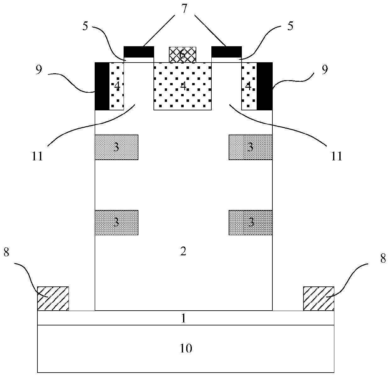
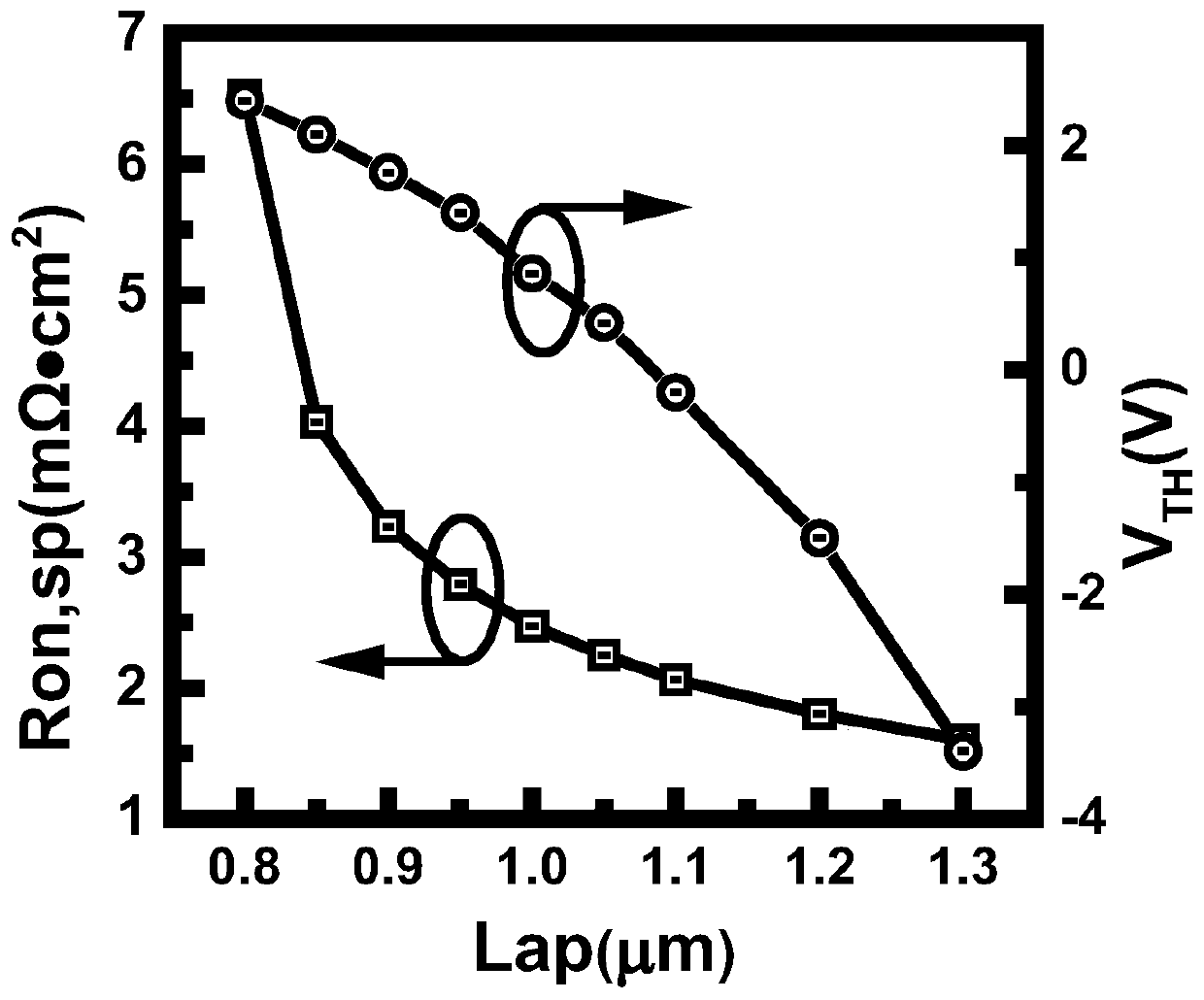
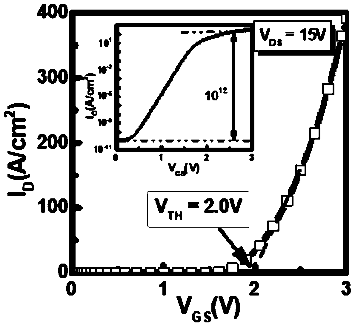
The invention belongs to the technical field of power semiconductors, and relates to a GaN longitudinal reverse conducting junction field effect transistor. Two back-to-back PN junctions on the top layer of a device are utilized to form a JFET structure to control opening and closing of a channel, and Schottky metal deposition is utilized to form an anode of a reverse conducting diode on P-GaN onone side. The threshold voltage of the device can be controlled by properly controlling the width of the channel and the doping concentration of the PN junction. Besides, a reverse biased PN junctionis introduced into a GaN drift region by a floating P-type GaN buried layer below the Schottky anode, and a depletion region of the reverse biased PN junction is continuously expanded when the reversebiased PN junction bears reverse withstand voltage so as to enable the electric field in the device body to be uniformly distributed, and the maximum peak electric field in the device can be effectively reduced. The beneficial effects are that the GaN longitudinal reverse conducting junction field effect transistor has the advantages of adjustable threshold voltage, low on-resistance, large saturation current, high off-state withstand voltage, low in power consumption and the like in a working state of the forward switch; and the GaN longitudinal reverse conducting junction field effect transistor has the advantages of low starting voltage, low conduction resistance, high reverse withstand voltage, low power consumption and the like in a reverse conduction working state.
Description
technical field [0001] The invention belongs to the technical field of power semiconductors, and relates to a GaN vertical reverse junction field effect transistor. Background technique [0002] As a representative of the third-generation wide-bandgap semiconductor materials, GaN is more and more widely used in today's society due to its material properties superior to those of the first-generation (Si) and second-generation (GaAs) semiconductor materials. Due to the large band gap and high power density of the GaN material, it plays an important role in 5G communication; the 2DEG at the AlGaN / GaN heterojunction interface due to the material polarization effect has a high concentration and high mobility. Features, so the device can achieve high switching frequency and low conduction loss, so this type of GaN device is widely used in driverless technology and electric vehicles. Compared with SiC materials, GaN, which also belongs to the third-generation semiconductor materia...
Claims
Login to View More Application Information
Patent Timeline
 Patent Type & AuthorityApplications(China)
IPC IPC(8): H01L29/78H01L29/06H01L29/20
CPCH01L29/0603H01L29/0615H01L29/0684H01L29/2003H01L29/78
Inventor周琦董志文魏鹏程马骁勇熊娓杨秀刘熙陈万军张波
OwnerUNIV OF ELECTRONICS SCI & TECH OF CHINA