
nor FLASH device structure and its manufacturing method

A technology of device structure and manufacturing method, which is applied in semiconductor/solid-state device manufacturing, semiconductor devices, electric solid-state devices, etc., can solve the problems of high process cost and process time, and achieve the effect of reducing process cost and process time

Active Publication Date: 2020-10-09
SHANGHAI HUALI MICROELECTRONICS CORP
View PDF3 Cites 0 Cited by
  • Summary
  • Abstract
  • Description
  • Claims
  • Application Information

AI Technical Summary

Problems solved by technology

[0009] In addition, customers have different requirements for different terminal applications, and have different requirements for the threshold voltage (VT) range in the erasing, programming or reading state, which will inevitably lead to corresponding process adjustments and long-term verification processes. Each terminal needs Both require customized products, which will result in higher process cost and process time in the application of multiple threshold voltages

Method used


Image

  • nor FLASH device structure and its manufacturing method

Examples


Embodiment Construction

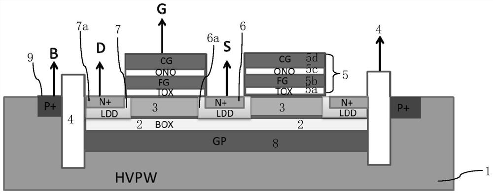
[0057] Such as figure 1 Shown is the device structure diagram of the NOR FLASH device structure of the embodiment of the present invention, and the NORFLASH device structure of the embodiment of the present invention includes:

[0058] An FDSOI substrate formed by sequentially stacking a bottom semiconductor substrate 1 , an insulating buried layer 2 and a top semiconductor substrate 3 .

[0059] In the embodiment of the present invention, the bottom semiconductor substrate 1 is a silicon substrate, the top semiconductor substrate 3 is a silicon substrate, and the buried insulating layer 2 is a buried silicon oxide layer. figure 1 In , the buried insulating layer 2 is also represented by BOX.

[0060] A shallow trench field oxygen 4 is formed on the FDSOI substrate, the shallow trench field oxygen 4 passes through the top semiconductor substrate 3 and the buried insulating layer 2, and the shallow trench field oxygen 4 The bottom enters into said bottom semiconductor substra...


PUM


Abstract

The invention discloses a NOR FLASH device structure, which includes: an FDSOI substrate, a plurality of active areas formed by top semiconductor substrates surrounded by shallow trench field oxygen, and multiple device unit structures formed in each active area. The device unit structure includes a source region, a drain region and a gate structure; a well region doped with a second conductivity type is formed in the bottom semiconductor substrate, and a second conductivity type doped well region is formed on the top surface of the corresponding well region at the bottom of each active region. The bottom field plate is composed of a conductive type doped region. In the outer area of ​​the active region, the surface of the well region is directly exposed and a heavily doped body extraction region of the second conductive type is formed on the surface of the exposed well region. The threshold voltage of each device unit structure can be adjusted by applying voltage to the body lead-out area. The invention discloses a method for manufacturing a NOR FLASH device structure. The invention can realize the adjustable threshold voltage of the device unit structure and can be applied to the application range of multiple threshold voltages under high process nodes.

Description

technical field [0001] The invention relates to the field of semiconductor integrated circuit manufacturing, in particular to a NOR (NOR) flash memory (FLASH) device structure. The present invention also relates to a manufacturing method of a NOR FLASH device structure Background technique [0002] Flash memory has been widely used as the best choice for non-volatile memory applications due to its advantages of high density, low price, and electrical programmability and erasability. [0003] With the inevitable trend of MOS process node improvement, it is imperative to reduce the size of the device cell structure (Cell) of each bit (Bit) of NOR FLASH; however, for NOR FLASH, problems such as power consumption and programming efficiency are becoming more and more serious due to size reduction. significantly. [0004] In the prior art, along with the shrinkage of the device size, a fully depleted (Fully Depleted, FD) semiconductor-on-insulator (Semiconductor On Insulator, SO...

Claims


Application Information

Patent Timeline
Patent Type & Authority Patents(China)
IPC IPC(8): H01L27/11524H01L21/762H01L27/12H10B41/35
Inventor 谈嘉慧彭宇飞
Owner SHANGHAI HUALI MICROELECTRONICS CORP
Learn More