Formation method of semiconductor structure

A technology in the direction of semiconductors and extensions, applied in semiconductor/solid-state device manufacturing, electrical components, circuits, etc., can solve the problems of difficult channels and poor channel control ability of the gate structure, and achieve large removal process window, Ease of removal, effect of improving density

Pending Publication Date: 2022-07-19
SEMICON MFG INT (SHANGHAI) CORP +1
View PDF0 Cites 0 Cited by
  • Summary
  • Abstract
  • Description
  • Claims
  • Application Information

AI Technical Summary

Problems solved by technology

However, as the channel length of the device is shortened, the distance between the source and the drain of the device is also shortened, so the ability of the gate structure to control the channel becomes worse, and the gate voltage pinches off the channel. The difficulty of the channel is also increasing, making the phenomenon of subthreshold leakage (subthreshold leakage), the so-called short-channel effect (short-channel effects, SCE) more prone to occur

Method used


Image

  • Formation method of semiconductor structure
  • Formation method of semiconductor structure
  • Formation method of semiconductor structure

Examples


Embodiment Construction

[0012] It can be known from the background art that the semiconductor structure formed at present still has the problem of poor electrical performance. Now combined with a method for forming a semiconductor structure, the reasons for the poor electrical performance of the semiconductor structure are analyzed.

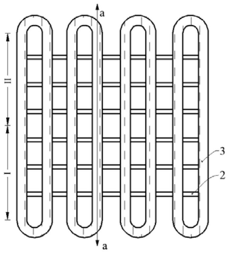
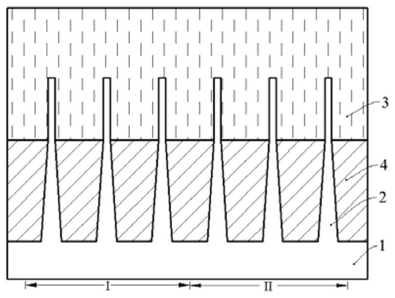
[0013] refer to Figure 1 to Figure 13 , a schematic diagram of the structure corresponding to each step in a method for forming a semiconductor structure is shown.

[0014] like figure 1 and figure 2 shown, figure 1 for a top view, figure 2 for figure 1 The cross-sectional view at aa, a base is provided, the base includes a substrate 1, a fin 2 separated from the substrate 1, an isolation layer 4 located on the fin 2 exposed on the substrate 1, and located on the The dummy gate structure 3 on the isolation layer 4 and across the fin portion 2 and the source and drain doped layers (not shown in the figure) in the fin portion 2 on both sides of the dummy gate s...


PUM


Abstract

A method for forming a semiconductor structure comprises the following steps: providing a substrate which comprises a first region and a second region, the substrate comprises a substrate body, fin parts separated on the substrate body, an isolation layer located on the fin parts and exposed out of the substrate body, a pseudo gate structure located on the isolation layer and crossing the fin parts, and an interlayer dielectric layer covering the side wall of the pseudo gate structure and exposed out of the top of the pseudo gate structure; removing the pseudo gate structure, and forming a gate opening in the interlayer dielectric layer; forming an annealing sacrificial layer in the gate opening; removing the annealing sacrificial layer; a mask layer with a first groove is formed, the extension direction of the first groove is the same as the extension direction of the fin part, and the first groove exposes a part of the gate opening at the junction of the first region and the second region; a first blocking layer is formed in the first recess. Therefore, the removal process window of the annealing sacrificial layer at the junction of the first region and the second region is relatively large, and residues are not easy to exist, so that the first gate structure and the second gate structure can better control the threshold voltage of the semiconductor structure.

Description

technical field [0001] Embodiments of the present invention relate to the field of semiconductor manufacturing, and in particular, to a method for forming a semiconductor structure. Background technique [0002] In semiconductor manufacturing, with the development trend of VLSI, the feature size of integrated circuits continues to decrease. In order to adapt to smaller feature sizes, Metal-Oxide-Semiconductor Field-Effect Transistor , MOSFET) channel length is correspondingly shortened. However, with the shortening of the channel length of the device, the distance between the source electrode and the drain electrode of the device is also shortened, so the control ability of the gate structure to the channel becomes worse, and the gate voltage pinch off the channel. The difficulty of channeling is also increasing, making the phenomenon of subthreshold leakage (subthreshold leakage), the so-called short-channel effects (SCE), more likely to occur. [0003] Therefore, in orde...

Claims


Application Information

Patent Timeline
Patent Type & Authority Applications(China)
IPC IPC(8): H01L21/8238
CPCH01L21/823821H01L21/823857H01L21/823828
Inventor 涂武涛王彦邱晶
Owner SEMICON MFG INT (SHANGHAI) CORP
Why Eureka
Try Eureka