LED packaging structure and packaging method thereof

A technology of LED packaging and packaging method, applied in electrical components, electrical solid devices, circuits, etc., can solve the problems of difficult to achieve automatic production, difficult to control packaging quality, loss of light output rate, etc., to achieve controllable quality, low production cost, The effect of increasing productivity

Inactive Publication Date: 2011-01-05
APT ELECTRONICS
View PDF5 Cites 21 Cited by
  • Summary
  • Abstract
  • Description
  • Claims
  • Application Information

AI Technical Summary

Problems solved by technology

But this encapsulation method that sticks the lens of injection molding on the surface of LED chip can produce the interface between lens and encapsulation material, and described interface will cause certain loss of light extraction rate; Problems such as light attenuation will also be caused by problems such as thermal mismatch; at the same time, this packaging method also has problems in the production process that are difficult to control the packaging quality and difficult to realize automatic production.

Method used


Image

  • LED packaging structure and packaging method thereof
  • LED packaging structure and packaging method thereof
  • LED packaging structure and packaging method thereof

Examples


Embodiment 1

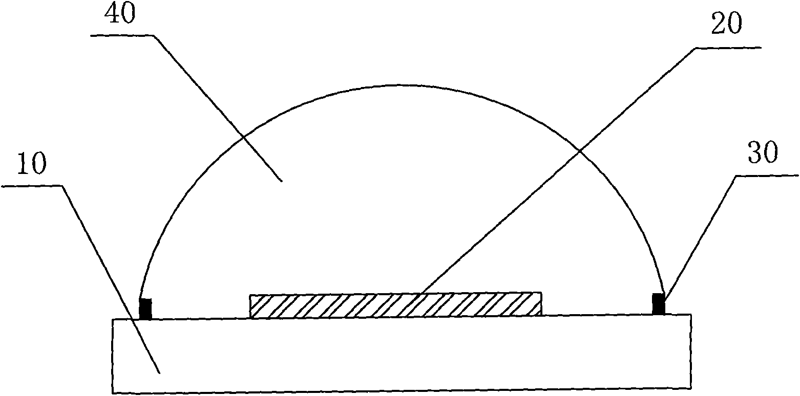
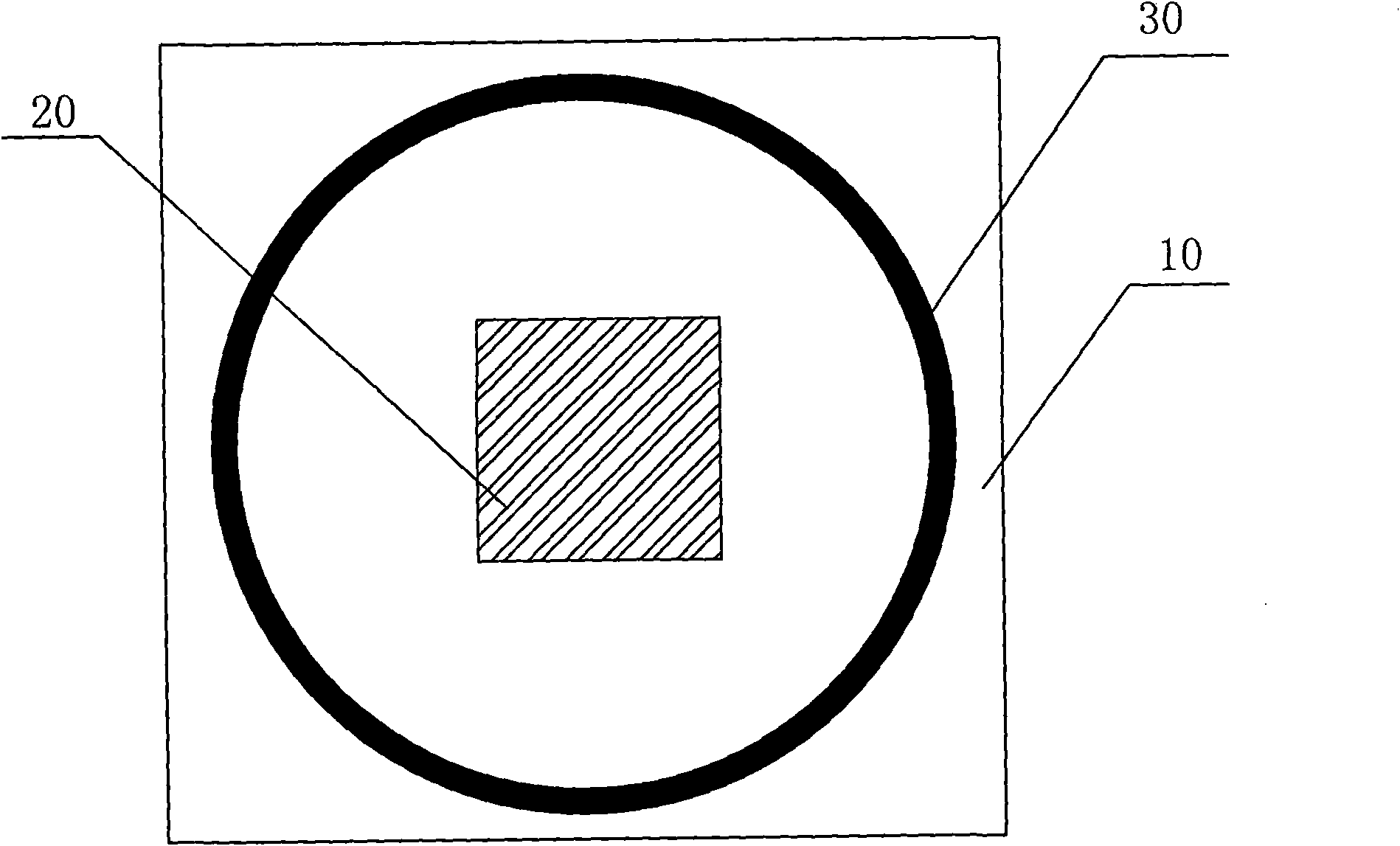
[0025] Please also see figure 1 and figure 2 ,in, figure 1 is a schematic cross-sectional view of the first embodiment of the LED packaging structure of the present invention, figure 2 yes figure 1 Top view of the LED package structure shown. The LED packaging structure includes a substrate 10 , an LED chip 20 , a convex wall 30 and a colloid lens 40 . The raised wall 30 is arranged on the substrate 10 to form a restricted area, and at least one LED chip 20 is arranged in the restricted area of ​​the raised wall 30 and fixed on the substrate 10 . The colloid lens 40 is arranged on the surface of the LED chip 20 and wraps the LED chip 20 inside.

[0026] Specifically, the substrate 10 may be a silicon wafer, a ceramic wafer, a printed circuit board (PCB), a metal-based printed circuit board (MCPCB), or a glass wafer.

[0027] The width of the convex wall 30 is 10um-5000um, and the height is 5um-5000um. The convex wall 30 can be circular arc ring, or polygonal ring, or ...

Embodiment 2

[0035] see Figure 5 and Figure 6 , Figure 5 is a schematic cross-sectional view of the second embodiment of the LED packaging structure of the present invention, Figure 6 yes Figure 5 Top view of the LED package structure shown. The LED packaging structure of the second embodiment is substantially the same as that of the first embodiment, the only difference being that an inner convex wall 32 and an outer convex wall 34 are arranged on the substrate 10, and the radius of the outer convex wall 34 is larger than that of the inner convex wall. 32 radius. One LED chip 20 is arranged in the restricted area of ​​the inner convex wall 32 and fixed on the substrate 10 . Wherein, the inner convex wall 32 is used for coating the phosphor powder layer 50 formed by the mixture of phosphor powder and silica gel, and the outer convex wall 34 is used for molding and encapsulating the colloidal lens 40 . Both the phosphor layer 50 and the colloidal lens 40 use the principle that th...

Embodiment 3

[0037] see Figure 7 and Figure 8 , Figure 7 is a schematic cross-sectional view of the third embodiment of the LED packaging structure of the present invention, Figure 8 yes Figure 7 Top view of the LED package structure shown. The LED packaging structure of the third embodiment is substantially the same as the LED packaging structure of the second embodiment, the only difference being that a plurality of LED chips 20 are arranged in the limited area of ​​the inner convex wall 32 and fixed on the substrate 10 . The sizes of the plurality of LED chips 20 may be the same, or may be a combination of chips of different sizes. The types of the plurality of LED chips 20 can also be different, and a multi-chip module can be composed of chips emitting different lights.

[0038]Compared with the prior art, the present invention can directly carry out the dispensing process on the LED chip to form the sealing lens, and at the same time, the structure of the convex wall is used...


PUM


Abstract

The invention relates to an LED packaging structure and a packaging method thereof. The LED packaging structure comprises a base plate, LED chips, one or more convex walls and a colloid lens molded under the restriction of the convex walls, wherein the convex walls are arranged on the base plate; at least one LED chip is arranged on the base plate in an area encircled by the convex walls; the area encircled by the convex walls is internally provided with the colloid lens for packaging the LED chip; and the colloid lens is formed by placing liquid colloid in the area restricted by the convex walls, utilizing the surface tension of the liquid to form a required colloid shape and carrying out solidification shaping. Compared with the prior art, the LED packaging structure of the invention is simple and reasonable, and the production process is simple and the cost is lower.

Description

technical field [0001] The invention belongs to the manufacturing field of photoelectric devices, and relates to an LED packaging structure and a manufacturing method thereof. Background technique [0002] Light-emitting diode (LED) light sources have the advantages of high efficiency, long life, and no harmful substances such as Hg. With the rapid development of LED technology, the brightness and lifespan of LEDs have been greatly improved, making the application of LEDs more and more extensive. From outdoor lighting such as street lamps to indoor lighting such as decorative lamps, they are all used or replaced one after another. into LED as light source. [0003] In the LED packaging structure, in order to improve the brightness of the LED and achieve better reliability, the surface of the LED is usually made of hemispherical or other shaped lenses using silica gel or epoxy resin to increase the light output of the LED. At present, the lens on the surface of the LED is m...

Claims


Application Information

Patent Timeline
Patent Type & Authority Applications(China)
IPC IPC(8): H01L33/48H01L33/52H01L33/58
CPCH01L33/54H01L25/0753H01L2933/005H01L2924/0002H01L2924/00
Inventor 阮承海曾照明陈海英肖国伟
Owner APT ELECTRONICS
Why Eureka
Try Eureka